Double-sided plug-in circuit board and manufacturing method

A manufacturing method and circuit board technology, applied in the directions of printed circuit manufacturing, printed circuits, printed circuit components, etc., can solve problems such as increased material cost, increased processing difficulty, and multiple circuit board spaces, and achieve a convenient processing and manufacturing method. Simple, simple processing effect

Inactive Publication Date: 2019-08-13
INSPUR SUZHOU INTELLIGENT TECH CO LTD
View PDF6 Cites 2 Cited by
  • Summary
  • Abstract
  • Description
  • Claims
  • Application Information

AI Technical Summary

Problems solved by technology

[0003] The crimping holes provided on both sides of the current circuit board are independent, that is, only one crimping hole can be set on the top or bottom of the circuit board at the same position, and the two crimping holes can only be arranged in a staggered manner. Different hole positions are set on the board, which will take up more space on the circuit board. In order to meet the quantity requirements of the crimping holes, the size and number of layers of the circuit board can only be increased, which will lead to an increase in material costs and processing difficulty. increase

Method used


Image

  • Double-sided plug-in circuit board and manufacturing method
  • Double-sided plug-in circuit board and manufacturing method
  • Double-sided plug-in circuit board and manufacturing method

Examples


Embodiment 1

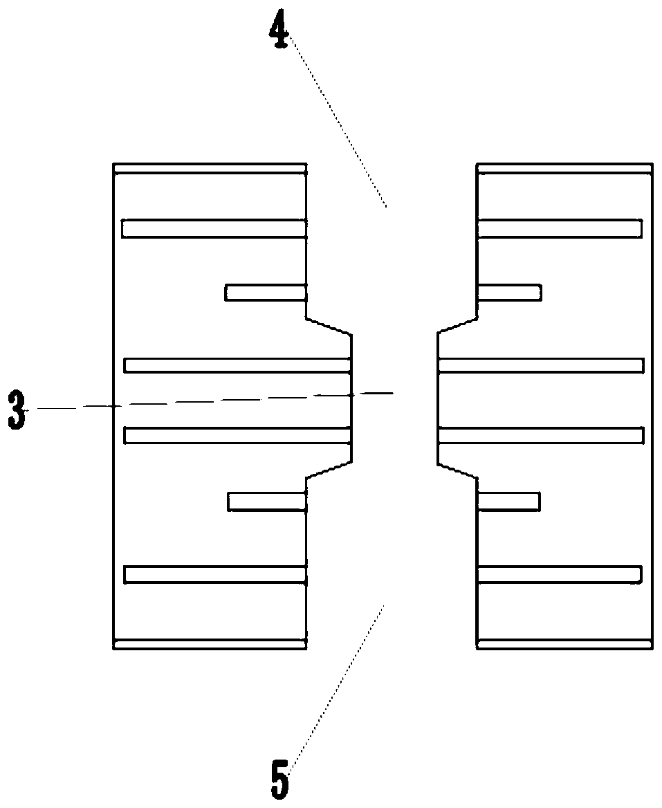
[0035] Such as Figure 5 As shown, a double-sided plug-in circuit board includes a circuit board body 1, and copper foil layers 2 parallel to each other are arranged in the circuit board body 1, and a first crimping is provided on one side of the circuit board body 1. hole 4, the other side of the circuit board body 1 is provided with a second crimping hole 5, the first crimping hole 4 corresponds to the second crimping hole 5, the first crimping hole 4 and the second crimping hole 5 The connecting holes 5 are connected through auxiliary holes 3 , and the inner walls of the first crimping hole 4 and the second crimping hole 5 are provided with electroplated copper 6 , and the electroplated copper 6 is connected with the copper foil layer 2 .

Embodiment 2

[0037] A method for manufacturing a double-sided plug-in circuit board, comprising the following steps:

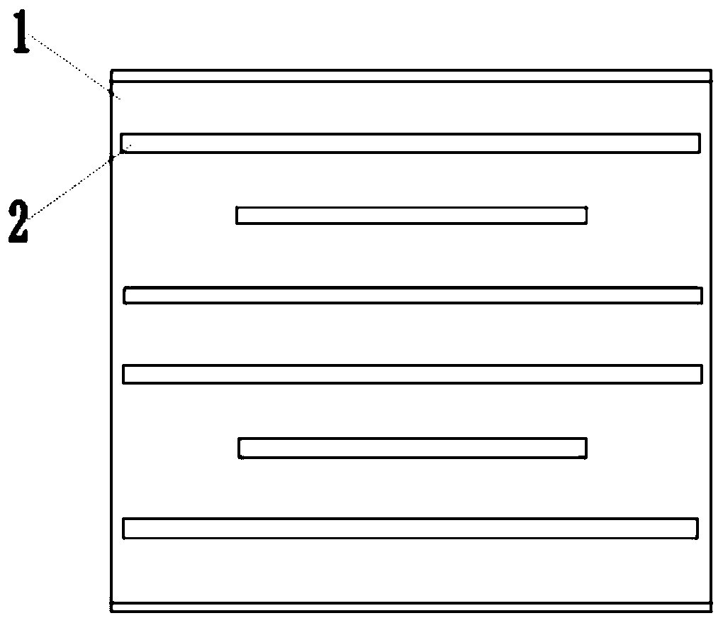
[0038] (1) if figure 1 As described above, the circuit board body 1 is designed with inner layer graphics and processed according to the inner layer graphics;

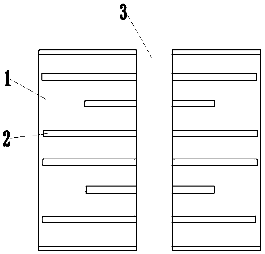
[0039] (2) if figure 2 As shown, an auxiliary hole 3 is drilled on the circuit board body 1, and the auxiliary hole 3 is a through hole;

[0040] (3) if image 3 As shown, a first crimping hole 4 is drilled on one side of the auxiliary hole 3, and a second crimping hole 5 is drilled on the other side of the auxiliary hole 3, and the first crimping hole 4 is connected with the second crimping hole. The diameters of the holes 5 are larger than the auxiliary holes 3. The diameter of the auxiliary holes 3 does not need to be too large, which is convenient for operation, fast drilling, and time-saving. On the other hand, it will not cause too much damage to the circuit board body 1, ensuring that the circuit board b...


PUM


Abstract

The invention discloses a double-sided plug-in circuit board and a manufacturing method thereof. The circuit board comprises a circuit board body, and copper foil layers which are parallel to each other are arranged in the circuit board body. One side of the circuit board body is provided with a first crimping hole, and the other side of the circuit board body is provided with a second crimping hole, wherein the position of the first crimping hole is corresponding to that of the second crimping hole, and the first crimping hole and the second crimping hole are connected through an auxiliary hole. The inner walls of the first crimping hole and the second crimping hole are provided with electroplated copper, and the electroplated copper is connected with the copper foil layer. The manufacturing method is simple, it is guaranteed that the crimping holes in the two sides can be electroplated through the auxiliary holes under the prior art condition. The machining technology is simple, themachining is convenient, and the cost is low; the crimping holes in the two sides are not communicated, are independent in use and do not affect each other, thereby saving the wiring space, and reducing the cost.

Description

technical field [0001] The invention relates to the technical field of circuit boards, in particular to a double-sided plug-in circuit board and a manufacturing method. Background technique [0002] In the printed circuit board industry, such as switch design, due to the increase in communication traffic in the information age, higher and higher requirements are placed on the communication traffic carried by network equipment, so the circuit boards of key components of equipment carry more and more There are many process designs, among which, for data transmission, more and more double-sided crimping design requirements are required, and the wiring space is getting smaller and smaller. [0003] The crimping holes provided on both sides of the current circuit board are independent, that is, only one crimping hole can be set on the top or bottom of the circuit board at the same position, and the two crimping holes can only be arranged alternately. Different hole positions are...

Claims


Application Information

Patent Timeline
Patent Type & Authority Applications(China)
IPC IPC(8): H05K1/11H05K3/42H05K3/00
CPCH05K1/115H05K3/0047H05K3/429
Inventor 宋玉娜
Owner INSPUR SUZHOU INTELLIGENT TECH CO LTD
Why Eureka
Try Eureka