Visible light wave band optical neural network element

A neural network and visible light technology, applied in the field of image recognition and optical components, can solve the problems of inability to work in the visible light band and low diffraction efficiency of diffractive components

Active Publication Date: 2019-08-16
苏州麦田光电技术有限公司
View PDF9 Cites 1 Cited by
  • Summary
  • Abstract
  • Description
  • Claims
  • Application Information

AI Technical Summary

Problems solved by technology

[0007] Aiming at the problem that the diffraction element processed by 3D printing method has low diffraction efficiency and cannot work in the visible light band, the present invention provides an optical neural network element, which uses substructures with the same size and different rotation angles to replace the different components in the diffraction element. High step structure, and the micro-nano processing method of single projection exposure, atomic layer deposition, etching process and slice segmentation can not only improve the diffraction efficiency, but also can work in the visible light band

Method used


Image

  • Visible light wave band optical neural network element
  • Visible light wave band optical neural network element
  • Visible light wave band optical neural network element

Examples


specific Embodiment 1

[0050] This embodiment is an embodiment of an optical neural network element in the visible light band.

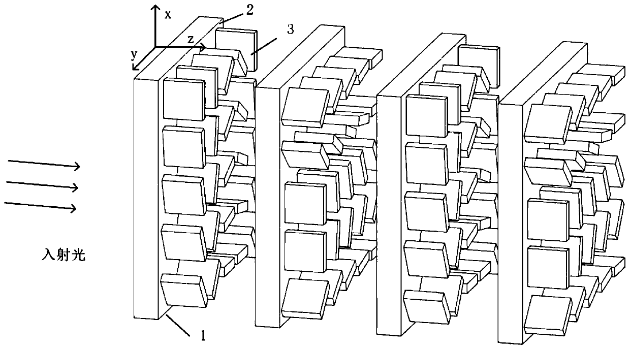
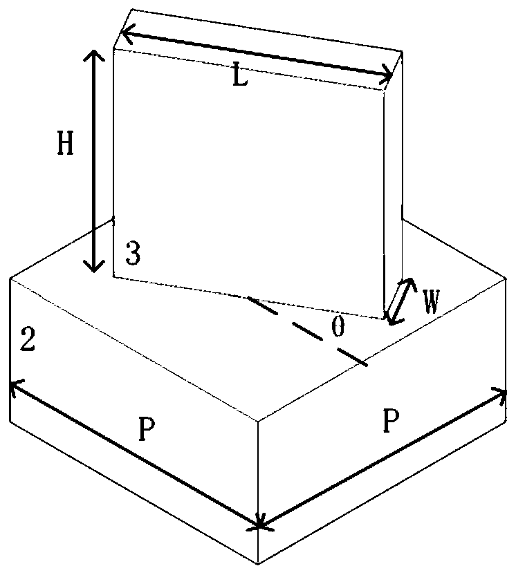
[0051] A visible light band optical neural network element of this embodiment, the structural diagram is as follows figure 1 shown. The optical neural network element in the visible light band is segmented through a single projection exposure, atomic layer deposition, etching process, and slice, and includes a plurality of subelements 1 arranged at equal intervals along the optical axis, and the subelements 1 are perpendicular to the The projection figure of the plane of the optical axis is a square, and the projection figures of all subcomponents 1 to the plane perpendicular to the optical axis coincide; each subcomponent 1 includes a substrate 2 and a plurality of substructures 3 supported by the substrate 2, such as figure 2 As shown, the substructures 3 are arranged in a matrix on the surface of the substrate 2. In the row direction and the column direction of the ma...

specific Embodiment 2

[0055] This embodiment is an embodiment of an optical neural network element in the visible light band.

[0056] An optical neural network element in the visible light band of this embodiment is further defined on the basis of the specific embodiment 1:

[0057] Define the incident light wavelength as λ d , the size (L, W, H) of each substructure 3 and the distance P between the coordinates of two adjacent substructures 3 on the substrate 2 form the parameter vector (L, W, H, P);

[0058] Wherein, L is the length of the substructure 3, W is the width of the substructure 3, and H is the height of the substructure 3;

[0059] The method for calculating substructure 3 parameter vectors (L, W, H, P) comprises the following steps:

[0060] Step a, assign a value to each parameter of (L, W, H, P), wherein the range of each parameter satisfies the following conditions: 0d and 100nmd , and each parameter is assigned an integer multiple of 5, and N L ×N W ×N H ×N P parameter ve...

specific Embodiment 3

[0072] This embodiment is an embodiment of an optical neural network element.

[0073] This embodiment is an embodiment of an optical neural network element in the visible light band.

[0074] An optical neural network element in the visible light band of this embodiment, on the basis of specific embodiment 1 or specific embodiment 2, further defines that the material of the substructure 3 is titanium dioxide or gallium nitride, and the material of the substrate 2 is silica.


PUM


Abstract

The invention discloses a visible light wave band optical neural network element, belonging to the technical field of optical elements and image recognition. The optical neural network element comprises a plurality of sub-elements orderly arranged with equal spacing along an optical axis direction, a projection figure of the sub-element on a plane perpendicular to the optical axis is square, the projection figures of all the sub-elements on the plane perpendicular to the optical axis are superposed; each sub-element contains one substrate structure and a plurality of substructures supported bythe substrate structure, the substructures are in matrix arrangement on a surface of the substrate, in a row direction and a column direction of the matrix, coordinate distance between two neighboring substructures on the substrate is a fixed value, the substructures are same in size and different in intersection angles, and the substructure intersection angle and phase in the sub-element have acertain determination relation. The visible light wave band optical neural network element not only is out of limit in diffraction efficiency, but also can work in a visible light wave band due to improvement of a processing technology; and the invention also provides a method of calculating substructure size.

Description

technical field [0001] The invention relates to an optical neural network element in the visible light band, which belongs to the technical field of optical elements and image recognition. Background technique [0002] In recent years, image recognition based on optical neural network has gradually developed. It is a combination of optical tools and neural network. Its principle is to simulate the working process of neurons with the propagation process of light, and express data information with light field intensity. Compared with The deep learning neural network based on electronic components has the advantages of fast speed, low energy consumption and easy interpretation of results. [0003] The article "All-optical machine learning using diffractive deep neural networks" involves an optical neural network used in the THz band. The optical neural network element is a type of diffractive element processed by 3D printing. It is characterized by different heights Step struc...

Claims


Application Information

Patent Timeline
Patent Type & Authority Applications(China)
IPC IPC(8): G02B5/18G02B27/00G06N3/067
CPCG02B5/1866G02B27/0012G02B2005/1804G06N3/067
Inventor 金光国
Owner 苏州麦田光电技术有限公司
Why Eureka
Try Eureka