Chip package structure

A chip packaging structure and chip technology, applied in the direction of electrical components, electrical solid devices, circuits, etc., to achieve the effect of increasing the contact area, achieving compatibility, and neutralizing thermal deformation

Pending Publication Date: 2019-08-16
JADE BIRD DISPLAY SHANGHAI LTD
View PDF0 Cites 4 Cited by
  • Summary
  • Abstract
  • Description
  • Claims
  • Application Information

AI Technical Summary

Problems solved by technology

However, whether the packaging structure can withstand different chip power and the heat dissipation between the packaging structure and the chip need to be further resolved.

Method used


Image

  • Chip package structure
  • Chip package structure
  • Chip package structure

Examples


Embodiment Construction

[0045] In order to make the content of the present invention clearer and easier to understand, the content of the present invention will be further described below in conjunction with the accompanying drawings. Of course, the present invention is not limited to this specific embodiment, and general replacements known to those skilled in the art are also covered within the protection scope of the present invention.

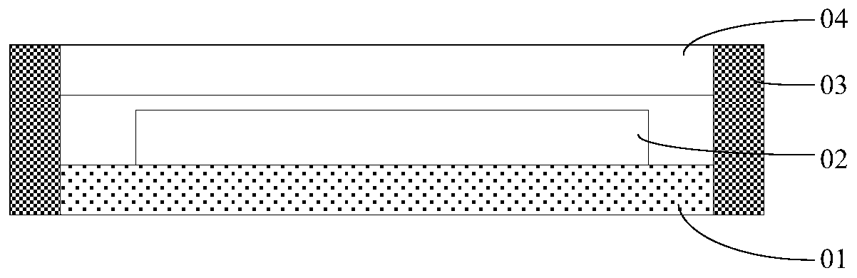
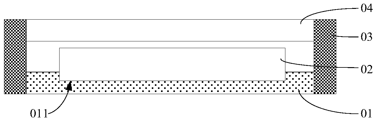
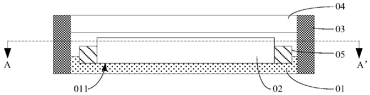
[0046] The chip packaging structure of the present invention comprises a circuit substrate, a chip on the circuit substrate, a packaging flat panel above the chip, and a sealing dam is used to seal the circuit substrate and the packaging flat panel.

[0047] The following is attached Figure 1-11 The present invention will be described in further detail with specific examples. It should be noted that the drawings are all in a very simplified form, using imprecise scales, and are only used to facilitate and clearly achieve the purpose of assisting in describing the...


PUM


Abstract

The invention provides a chip package structure, the gap between a circuit substrate and a package plate is sealed by a sealing dam, and therefore, the package of a chip is achieved. Further, a recessis set in the circuit substrate to insert the chip into the recess, so the positions of the circuit substrates and the chips can be accurately determined, the bonding area between the chip and the circuit substrate is increased, and therefore, the stability of the chip package and the thermal conductivity between the chip and the circuit substrate is improved. A thermal conductive gasket is used,the heat dissipation of the chip is promoted, and the thermal deformation between the chip and the circuit substrate can be neutralized. When the chip is expanded due to heat, the contact area between the chip and the thermal conductive gasket is increased, the heat transfer amount is increased, the collision caused by the direct rigid contact of the chip with the circuit substrate is avoided, and the crushing stress borne by the chip is reduced.

Description

technical field [0001] The invention relates to the technical field of semiconductor packaging, in particular to a chip packaging structure. Background technique [0002] Semiconductor chip packaging refers to the housing used to install semiconductor chips. It not only plays the role of placing, fixing, sealing, protecting new chips and enhancing thermal conductivity, but also serves as a bridge to communicate with the internal and external circuits of the chip. Usually, the wires on the chip are connected to the pins of the package shell, and the pins are electrically connected to other devices through the lines on the printed circuit board. Therefore, the packaging structure plays a very important role in the chip. With the development of technology, the requirements for the ratio of chip packaging area to chip area, applicable frequency, temperature resistance, weight, reliability, portability and other performance are getting higher and higher, resulting in chip packag...

Claims


Application Information

Patent Timeline
Patent Type & Authority Applications(China)
IPC IPC(8): H01L33/54H01L33/48H01L33/44H01L33/64H01L23/00
CPCH01L23/562H01L33/44H01L33/48H01L33/483H01L33/54H01L33/641H01L33/642
Inventor 季懿栋琚晶徐晨超李起鸣
Owner JADE BIRD DISPLAY SHANGHAI LTD
Why Eureka
Try Eureka