Pixel defining layer and manufacturing method thereof, display panel and manufacturing method thereof and display device

A technology of pixel definition layer and fabrication method, applied in semiconductor/solid-state device manufacturing, electrical components, electrical solid-state devices, etc., can solve problems such as affecting the uniformity of ink film formation

Active Publication Date: 2019-08-23
BOE TECH GRP CO LTD
View PDF4 Cites 4 Cited by
  • Summary
  • Abstract
  • Description
  • Claims
  • Application Information

AI Technical Summary

Problems solved by technology

However, due to the difference in surface energy at the surface where the ink contacts the pixel defining layer, or the drying characteristics of the ink, etc., the ink of inkjet printing will climb to a certain extent on the side surface of the pixel defining layer, thereby affecting the surface of the pixel defining layer. Uniformity of ink film formation within the pixel area

Method used


Image

  • Pixel defining layer and manufacturing method thereof, display panel and manufacturing method thereof and display device
  • Pixel defining layer and manufacturing method thereof, display panel and manufacturing method thereof and display device
  • Pixel defining layer and manufacturing method thereof, display panel and manufacturing method thereof and display device

Examples


Embodiment Construction

[0047] In order to illustrate the present invention more clearly, the present invention will be further described below in conjunction with preferred embodiments and accompanying drawings. Similar parts in the figures are denoted by the same reference numerals. Those skilled in the art should understand that the content specifically described below is illustrative rather than restrictive, and should not limit the protection scope of the present invention.

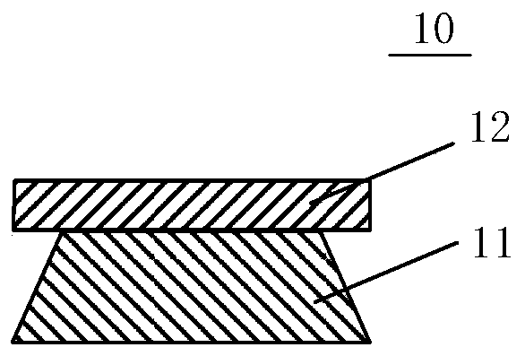
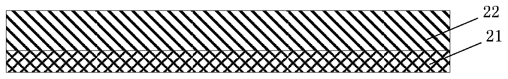
[0048] like figure 1 As shown, an embodiment of the present invention provides a pixel defining layer, including a first pixel defining layer disposed on a substrate; a second pixel defining layer located on a side of the first pixel defining layer away from the substrate, The orthographic projection of the surface of the second pixel defining layer close to the substrate on the substrate covers the orthographic projection of the surface of the first pixel defining layer far away from the substrate on the substrate, and th...


PUM


Abstract

The invention discloses a pixel defining layer and a manufacturing method thereof, a display panel and a manufacturing method thereof and a display device. The pixel defining layer comprises a first pixel defining layer arranged on a substrate; a second pixel defining layer located at the side of the first pixel defining layer away from the substrate, wherein the orthographic projection of the surface of the second pixel defining layer close to the substrate on the substrate covers the orthographic projection of the surface of the first pixel defining layer away from the substrate on the substrate, and the second pixel defining layer is made of hydrophobic material. Ink climbing on the pixel defining layer can be effectively suppressed, the electric leakage risk of the device layer of theorganic light emitting diode can be reduced and the film formation uniformity can be improved.

Description

technical field [0001] The present invention relates to the field of display technology, in particular to a pixel defining layer and a manufacturing method, a display panel and a manufacturing method, and a display device. Background technique [0002] Compared with LCD, Organic Light-Emitting Diode (OLED) has the advantages of self-luminescence, fast response, wide viewing angle, high brightness, bright color, light and thin, etc., and is considered to be the next generation display technology. [0003] The thin film deposition methods of organic material films for organic electroluminescent devices mainly include vacuum evaporation and solution process: 1. Vacuum evaporation is suitable for small organic molecules. Its film formation is uniform and the technology is relatively mature, but the investment in equipment is large. 1. Low material utilization rate and low alignment accuracy of large-sized products; 2. Solution process, including spin coating, inkjet printing, no...

Claims


Application Information

Patent Timeline
Patent Type & Authority Applications(China)
IPC IPC(8): H01L27/32H01L51/56
CPCH10K59/122H10K71/00
Inventor 侯文军
Owner BOE TECH GRP CO LTD
Why Eureka
Try Eureka