Pixel defining layer, display substrate and manufacturing method, display device

A technology of pixel definition layer and display substrate, which is applied in semiconductor devices, electrical components, circuits, etc., can solve the problems affecting the uniformity of solution film formation, and achieve the effect of reducing film formation uniformity and impact.

Active Publication Date: 2020-05-26
BOE TECH GRP CO LTD
View PDF3 Cites 0 Cited by
  • Summary
  • Abstract
  • Description
  • Claims
  • Application Information

AI Technical Summary

Problems solved by technology

[0005] Embodiments of the present invention provide a pixel defining layer, a display substrate, a manufacturing method, and a display device, which can solve the problem that the inkjet printing solution in the related art will climb to a certain extent on the side surface of the pixel defining layer, thereby affecting the The uniformity of the film formation of the solution in the pixel area

Method used


Image

  • Pixel defining layer, display substrate and manufacturing method, display device
  • Pixel defining layer, display substrate and manufacturing method, display device
  • Pixel defining layer, display substrate and manufacturing method, display device

Examples


Embodiment Construction

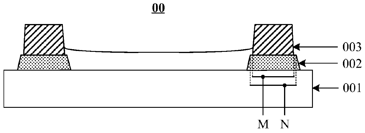
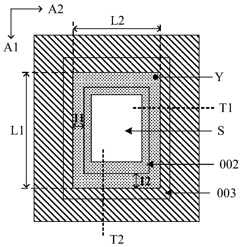
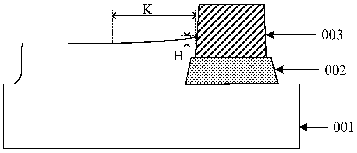
[0053] In order to make the object, technical solution and advantages of the present invention clearer, the implementation manner of the present invention will be further described in detail below in conjunction with the accompanying drawings.

[0054] Compared with liquid crystal displays, OLED displays have the advantages of self-illumination, fast response, wide viewing angle, high brightness, bright colors and thinness. There are mainly two methods for manufacturing the film layer in organic electroluminescent devices: vacuum evaporation and solution process. Vacuum evaporation is suitable for the film formation of organic small molecule materials. It has the advantages of good film formation uniformity and relatively mature technology. However, its film formation equipment has large investment, low material utilization rate and alignment accuracy when used for large-scale products. Low. The solution process includes methods such as spin coating, inkjet printing and nozzle...


PUM

PropertyMeasurementUnit
thicknessaaaaaaaaaa

Abstract

The invention discloses a pixel defining layer, a display substrate, a manufacturing method, and a display device, belonging to the field of display. The pixel defining layer includes: a lyophilic material layer arranged on the base substrate, and a lyophobic material layer arranged on the side of the lyophilic material layer away from the base substrate; the lyophobic material layer is close to the The orthographic projection of the surface of the base substrate on the base substrate is located within the orthographic projection of the surface of the lyophilic material layer away from the base substrate on the base substrate; wherein, the lyophilic material The layer is made of a lyophilic material, the lyophilic material is a material that is attractive to a solution in which the organic electroluminescent material is dissolved, and the lyophobic material layer is made of a lyophobic material, and the lyophobic material is The solution in which the organic electroluminescent material is dissolved has a repellent material. The invention reduces the influence of solution climbing on the film-forming uniformity of the solution in the pixel area. The invention is used for manufacturing display substrates of organic light emitting diodes.

Description

technical field [0001] The invention relates to the display field, in particular to a pixel defining layer, a display substrate, a manufacturing method, and a display device. Background technique [0002] An organic light-emitting diode (English: Organic Light-Emitting Diode; abbreviation: OLED) display panel includes an anode, a hole injection layer, a hole transport layer, an organic material film layer, an electron transport layer, an electron injection layer, and a cathode. Wherein, the organic material film layer can be manufactured by inkjet printing technology. When using inkjet printing technology to manufacture organic material film layers, it is necessary to form a pixel-defining layer on the base substrate, and then spray the solution of dissolving organic light-emitting materials onto the base substrate on which the pixel-defining layer is formed to form an organic material. film layer. [0003] In the related art, the pixel defining layer is generally made of ...

Claims


Application Information

Patent Timeline
Patent Type & Authority Patents(China)
IPC IPC(8): H01L27/32
CPCH10K59/352H10K59/122H10K71/13H10K59/35H10K71/00H10K71/135H10K59/1201
Inventor 侯文军
Owner BOE TECH GRP CO LTD
Why Eureka
Try Eureka