

Preparation method of display substrate, display substrate and display device
A technology of display substrate and display area, applied in branch equipment, organic semiconductor devices, semiconductor devices, etc., can solve the problems of lower reliability of display products, more holes in the display area, and packaging failure.
- Summary
- Abstract
- Description
- Claims
- Application Information
AI Technical Summary
Problems solved by technology
Method used
Image

Examples
Embodiment Construction
[0029] In order to make the above objects, features and advantages of the present invention more comprehensible, the present invention will be further described in detail below in conjunction with the accompanying drawings and specific embodiments.
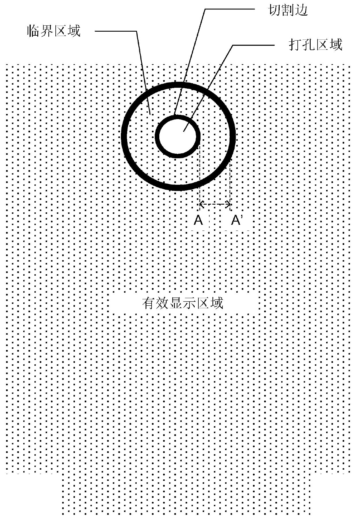
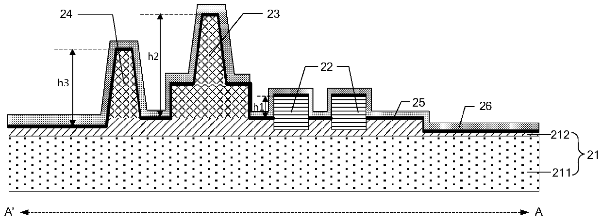
[0030] The inventors found that, in order to punch a hole in the display area, the crack formed during the cutting process is related to the thickness of the inorganic layer at the cutting edge. In the process of depositing the film layer, masks such as CVD (Chemical Vapor Deposition, Chemical Vapor Deposition) Mask cannot support and block the perforated area, so the inorganic film layer deposited by CVD will extend from the effective display area to the hole. The cutting edge increases the thickness of the inorganic film layer on the cutting edge, which makes it easy to generate cracks during the cutting process, and then the cracks extend to the effective display area in the subsequent process, resulting in package failure.
[...
PUM
 Abstract
Description
Claims
Application Information