An anti-bridging chip pin

A technology of pins and chips, which is applied in the direction of semiconductor/solid-state device parts, semiconductor devices, electrical components, etc., can solve the problems of low solderability and reduced solderability, etc., to strengthen the tin on the pins and reduce the probability of contact , the effect of increasing the thickness

Active Publication Date: 2021-03-02
INSPUR SUZHOU INTELLIGENT TECH CO LTD
View PDF1 Cites 0 Cited by
  • Summary
  • Abstract
  • Description
  • Claims
  • Application Information

AI Technical Summary

Problems solved by technology

[0003] The utility model aims to solve the above-mentioned deficiencies in the prior art, and provides an anti-bridging chip pin. The tin hole can ensure that the excess solder climbs along the inner side of the tin hole during welding, and a part of the excess solder can be accommodated. One side of the solder pin is nickel-plated and the other side is not plated. There will be a passivation film on the surface of the nickel-plated layer, which reduces the solderability. When the chip pins are placed on the solder paste, the bottom of the nickel-plated layer contacts first The main board, and then squeeze the excess solder paste along the tin guide slope to the smooth surface and the tin hole. There will be no solder paste squeezed out on the side of the nickel plating layer, so that the smooth surface can climb tin normally, and the solder extruded from the smooth side The paste flows to the adjacent nickel plating layer. Since there will be a passivation film on the surface, the solderability will be reduced very low, and there will be no bridging phenomenon.

Method used


Image

  • An anti-bridging chip pin
  • An anti-bridging chip pin
  • An anti-bridging chip pin

Examples


Embodiment Construction

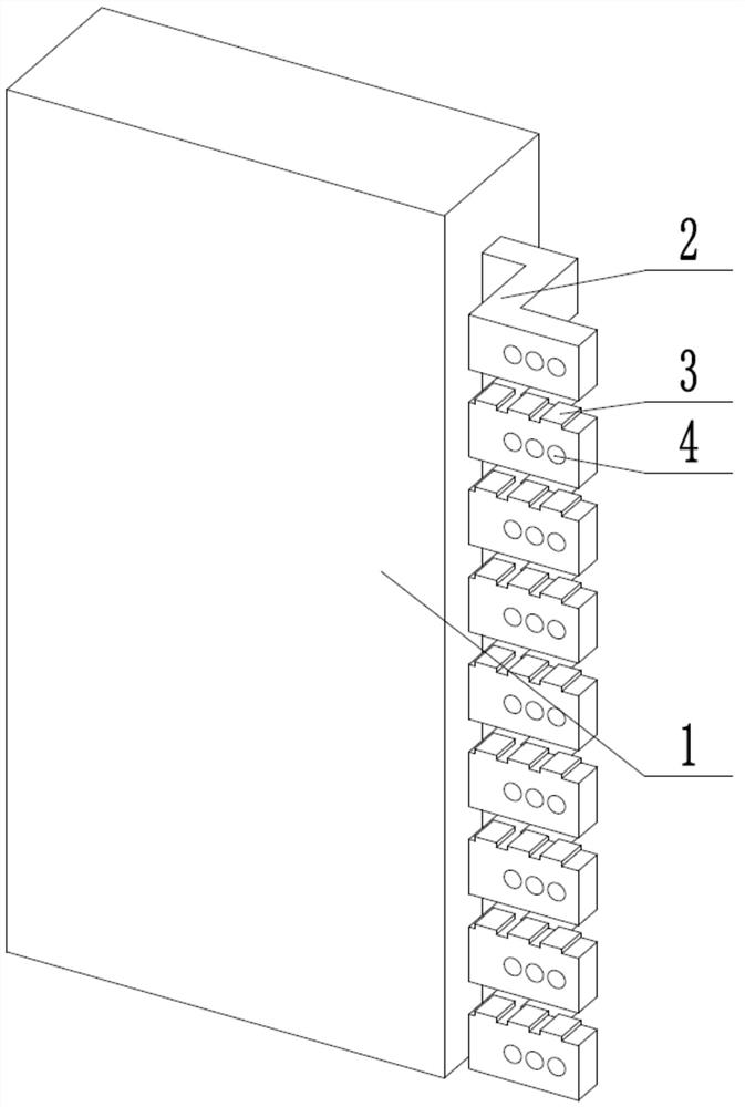
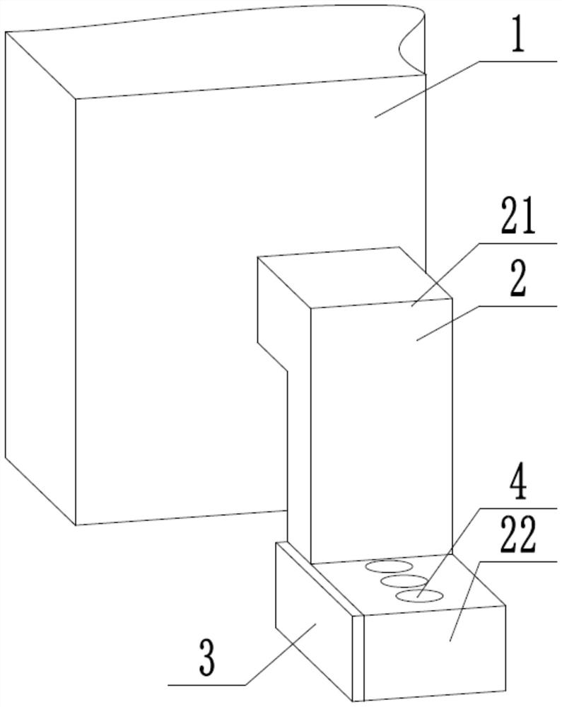
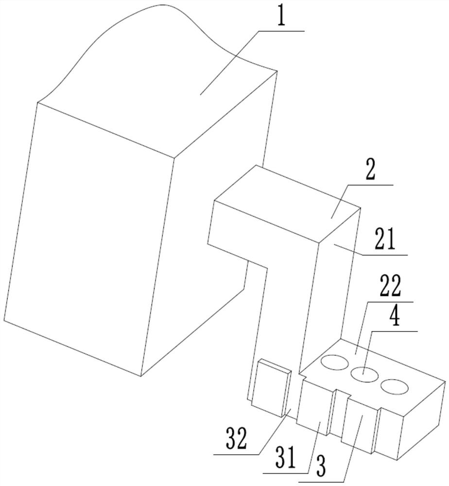
[0021] In order to clearly illustrate the technical features of this solution, the utility model will be described in detail below through specific implementation methods and in conjunction with the accompanying drawings. The following disclosure provides many different embodiments or examples for realizing different structures of the present invention. To simplify the disclosure of the present invention, components and arrangements of specific examples are described below. Furthermore, the present invention may repeat reference numerals and / or letters in different instances. This repetition is for the purpose of simplicity and clarity and does not in itself indicate a relationship between the various embodiments and / or arrangements discussed. It should be noted that components illustrated in the figures are not necessarily drawn to scale. The present invention omits descriptions of known components and processing techniques and processes to avoid unnecessarily limiting the ...


PUM


Abstract

The invention discloses an anti-bridging chip pin, which includes a chip body and pins, a plurality of pins arranged side by side on the edge of the chip body, and also includes a nickel plating layer and tin holes. The pins include supporting feet, welding feet, supporting The pins are connected to the chip body and the soldering pins, and the soldering pins are connected to the main board through soldering tin. The tin holes are set on the soldering surface of the soldering pins. The tin holes can ensure that the excess solder climbs along the inner side of the tin hole during soldering, and store a part of the excess solder. At the same time, one side of the solder pin is nickel-plated and the other side is not plated. There will be a passivation film on the surface of the nickel-plated layer, which reduces the solderability. When the chip pins are placed on the solder paste, the bottom of the nickel-plated layer Contact the motherboard first, and then squeeze the excess solder paste along the tin guide slope to the smooth surface and tin holes. There will be no solder paste squeezed out from the side of the nickel plating layer, and the solder paste squeezed out from the smooth side will flow to the adjacent solder paste. Nickel plating layer, because there will be a passivation film on the surface, the solderability is very low, and there will be no bridging phenomenon.

Description

technical field [0001] The utility model relates to the technical field of pin welding, in particular to a bridge-proof chip pin. Background technique [0002] Most of the components on the computer motherboard have pins, and most of them are surface mount. In practical applications, when these parts with pins are produced on the surface mount, because the pins have a certain width and height and are arranged closely, and the solder paste is just below the pins, when the amount of solder paste is too large When it is used, it often happens that the pin squeezes the solder paste between the two pins, causing the soldering problem of bridging between the two pins, which will cause a short circuit between the pins of the part, resulting in the part not working properly. The patent (application number: 201510564396.7) discloses a pin structure with only a through-hole structure. During actual soldering, solder will still be squeezed out between the pins, resulting in bridging. ...

Claims


Application Information

Patent Timeline
Patent Type & Authority Patents(China)
IPC IPC(8): H01L23/498
CPCH01L23/498H01L23/49894
Inventor 马亚辉于浩
Owner INSPUR SUZHOU INTELLIGENT TECH CO LTD
Why Eureka
Try Eureka