A sawtooth smoothing method for via array

A technology of via array and hole array, which is applied in the field of PCB simulation, can solve the problems of difficult comparison between test accuracy and simulation accuracy, time rises exponentially, and graphics algorithm redundancy, etc., so as to reduce simulation time, reduce complexity, Reduce the effect of vertices

Active Publication Date: 2022-03-22
XPEEDIC CO LTD
View PDF8 Cites 0 Cited by
  • Summary
  • Abstract
  • Description
  • Claims
  • Application Information

AI Technical Summary

Problems solved by technology

[0004] In PCB via hole simulation, for via hole design, a large-scale via hole array is generally displayed in RFIC (radio frequency integrated circuit), and the production process and uniform heating requirements are considered during production, but in the field of simulation , this kind of large-scale via array usually presents millions of orders of magnitude or more, which causes structural complexity and redundancy of graphic algorithms, and affects the simulation accuracy, making the simulation time increase exponentially, which is very difficult for manufacturers to obtain RFIC. The comparison between the test accuracy of the model and the simulation accuracy is extremely difficult
To sum up, the simulation time caused by large-scale via arrays in the prior art is long and the simulation accuracy is not high. The above problems are problems that need to be solved urgently in the prior art

Method used


Image

  • A sawtooth smoothing method for via array
  • A sawtooth smoothing method for via array
  • A sawtooth smoothing method for via array

Examples


Embodiment 1

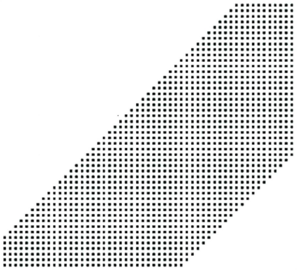
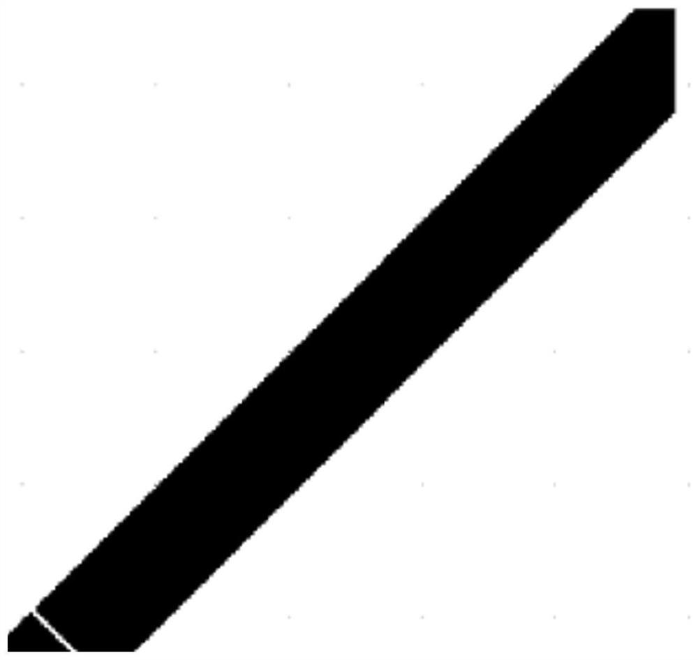
[0029] to combine figure 1 As shown, a zigzag smoothing method for a via array of the present invention first obtains the layout information of the PCB. It is worth noting that the attribute information of all via patterns on the layout can be obtained by scanning the PCB; further, for the via The arrays are classified, and then the via arrays are merged according to the arrangement of the via arrays; then the vias are classified according to the connection relationship between the vias and the layer, and the classified vias are merged; and then sequentially selected The vertex of the via hole, and judge whether the selected vertex is collinear with the two adjacent vertices. If the selected vertex is collinear with the two adjacent vertices, the selected vertex and the adjacent two vertices will be The two vertices are connected into a straight line. It is worth noting that the vertices refer to the small points that form the via hole graphics (such as figure 2 shown).

[...


PUM


Abstract

The invention discloses a sawtooth smoothing method for a via hole array, which belongs to the field of PCB simulation. A sawtooth smoothing method for a via array of the present invention first obtains the layout information of the PCB, then classifies the via array, and merges the via array according to the arrangement of the via array; then according to the via and the layer Classify the vias according to the connection relationship, and merge the classified vias; then select the vertices of the vias in turn, and judge whether the selected vertices and the two adjacent vertices are collinear, if the selected vertices and If the two adjacent vertices are collinear, connect the selected vertex and the two adjacent vertices into a straight line. The purpose of the present invention is to overcome the shortcoming of long simulation time caused by large-scale via arrays in the prior art, and provides a sawtooth smoothing method for via arrays, which can shorten the simulation time, thereby improving work efficiency, and further can Improve the accuracy of the simulation.

Description

technical field [0001] The invention relates to the field of PCB simulation, in particular to a sawtooth smoothing method for via hole arrays. Background technique [0002] PCB (Printed Circuit Board) is called a printed circuit board, also known as a printed circuit board. It is an important electronic component, a support for electronic components, and a carrier for electrical connections of electronic components. Because it is made using electronic printing, it is called a "printed" circuit board. PCB includes via holes, blind holes and buried holes. Via holes are also called through holes, which are all opened from the top layer to the bottom layer. In a four-layer PCB, the via holes run through layers 1, 2, 3, and 4, right? Coherent layer routing will be hindered; blind holes can only be seen on one of the top or bottom layers, and the other layer cannot be seen, that is to say, blind holes are drilled from the surface, but not through all layers; Buried hole refers t...

Claims


Application Information

Patent Timeline
Patent Type & Authority Patents(China)
IPC IPC(8): G06F30/398G06F115/12
CPCG06F30/20
Inventor 沈叶锋凌峰蒋历国代文亮张进军陈华
Owner XPEEDIC CO LTD
Why Eureka
Try Eureka