Display panel and manufacturing method thereof, and intelligent terminal

A technology for display panels and manufacturing methods, applied in semiconductor/solid-state device manufacturing, electrical components, diodes, etc., can solve problems such as poor light transmittance of display screens, achieve improved light transmittance, increase light transmittance area, The effect of increasing the amount of light

Active Publication Date: 2019-08-30
WUHAN CHINA STAR OPTOELECTRONICS SEMICON DISPLAY TECH CO LTD
View PDF6 Cites 5 Cited by
  • Summary
  • Abstract
  • Description
  • Claims
  • Application Information

AI Technical Summary

Problems solved by technology

[0004] An embodiment of the present invention provides a display panel to solve the problem of poor light transmittance of existing display screens

Method used


Image

  • Display panel and manufacturing method thereof, and intelligent terminal
  • Display panel and manufacturing method thereof, and intelligent terminal
  • Display panel and manufacturing method thereof, and intelligent terminal

Examples


Embodiment Construction

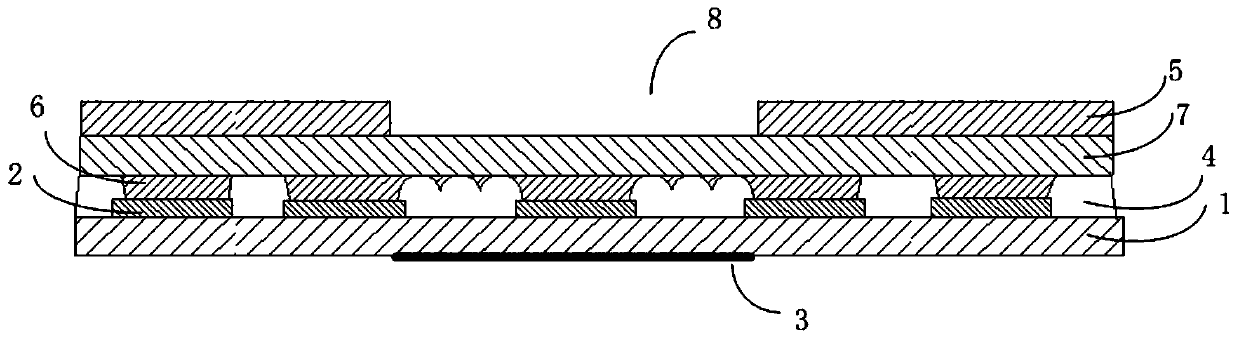
[0037] The preferred embodiments of the present invention are introduced below with reference to the accompanying drawings, in order to prove that the present invention can be implemented, and these embodiments can completely introduce the technical content of the present invention to those skilled in the art, so that the technical content of the present invention is more clear and easy to understand. However, the present invention can be embodied in many different forms of embodiments, and the protection scope of the present invention is not limited to the embodiments mentioned herein.

[0038] Terms used in the description of the present invention are used to describe specific embodiments only, and are not intended to show the concept of the present invention. Expressions used in the singular encompass expressions in the plural unless there is a clearly different meaning in the context. In the description of the present invention, it should be understood that terms such as ...


PUM


Abstract

The invention discloses a display panel and a manufacturing method thereof, and an intelligent terminal. The display panel includes a light sensing region used for disposing a light sensor of a camera, the display panel includes an array substrate and an anode arranged on the array substrate, wherein the light sensing region is arranged at one side of the array substrate away from the anode, the anode corresponding to the light sensing region is a patterned structure, and thereby light transmittance of the display panel is improved.

Description

technical field [0001] The present invention relates to the technical field of display panels, in particular to a display panel, a manufacturing method thereof, and an intelligent terminal. Background technique [0002] Compared with liquid crystal displays, active-matrix organic light-emitting diode (AMOLED) displays have the advantages of high contrast, high viewing angle, and fast response to moving images, and are increasingly used on smartphone screens. In order to ensure the maximum visual effect of smartphones, vigorously develop full-screen smartphones. [0003] At present, the camera in a full-screen smartphone is generally placed under the screen (CUP), but the base polyimide (PI) film layer of the display screen, the metal film layer in the array layer, the anode, the organic functional film layer, the cathode, the film The encapsulation layer, polarizer, etc. affect the transmittance of light passing through the screen, among which the PI film layer, anode, pola...

Claims


Application Information

Patent Timeline
Patent Type & Authority Applications(China)
IPC IPC(8): H01L27/32H01L51/52
CPCH10K59/65H10K59/122H10K50/81H10K50/813H10K50/85H10K71/00H10K50/818H10K59/1201
Inventor 夏存军
Owner WUHAN CHINA STAR OPTOELECTRONICS SEMICON DISPLAY TECH CO LTD
Why Eureka
Try Eureka