OLED display panel and manufacturing method thereof

A technology for display panels and manufacturing methods, applied in semiconductor/solid-state device manufacturing, photovoltaic power generation, electrical components, etc., can solve problems such as water vapor ingress, and the side walls of panel openings are not effectively protected, so as to ensure packaging reliability and improve Light transmittance to ensure clear imaging effect

Inactive Publication Date: 2019-09-10
WUHAN CHINA STAR OPTOELECTRONICS SEMICON DISPLAY TECH CO LTD
View PDF5 Cites 16 Cited by
  • Summary
  • Abstract
  • Description
  • Claims
  • Application Information

AI Technical Summary

Problems solved by technology

[0004] The invention provides an OLED display panel and a manufacturing method thereof, so as to solve the problem in the prior art that the sidewall of the panel opening is not effectively protected, causing water vapor to enter the OLED device

Method used


Image

  • OLED display panel and manufacturing method thereof
  • OLED display panel and manufacturing method thereof
  • OLED display panel and manufacturing method thereof

Examples


Embodiment Construction

[0036] The following descriptions of the various embodiments refer to the accompanying drawings to illustrate specific embodiments in which the invention may be practiced. The directional terms mentioned in the present invention, such as [top], [bottom], [front], [back], [left], [right], [inside], [outside], [side], etc., are only for reference The orientation of the attached schema. Therefore, the directional terms used are used to illustrate and understand the present invention, but not to limit the present invention. In the figures, structurally similar elements are denoted by the same reference numerals.

[0037] The present invention aims at the technical defect that water vapor invades into the OLED panel due to the need to open holes on the display panel, but the side of the display panel opening is not completely protected, and this solution can solve this defect.

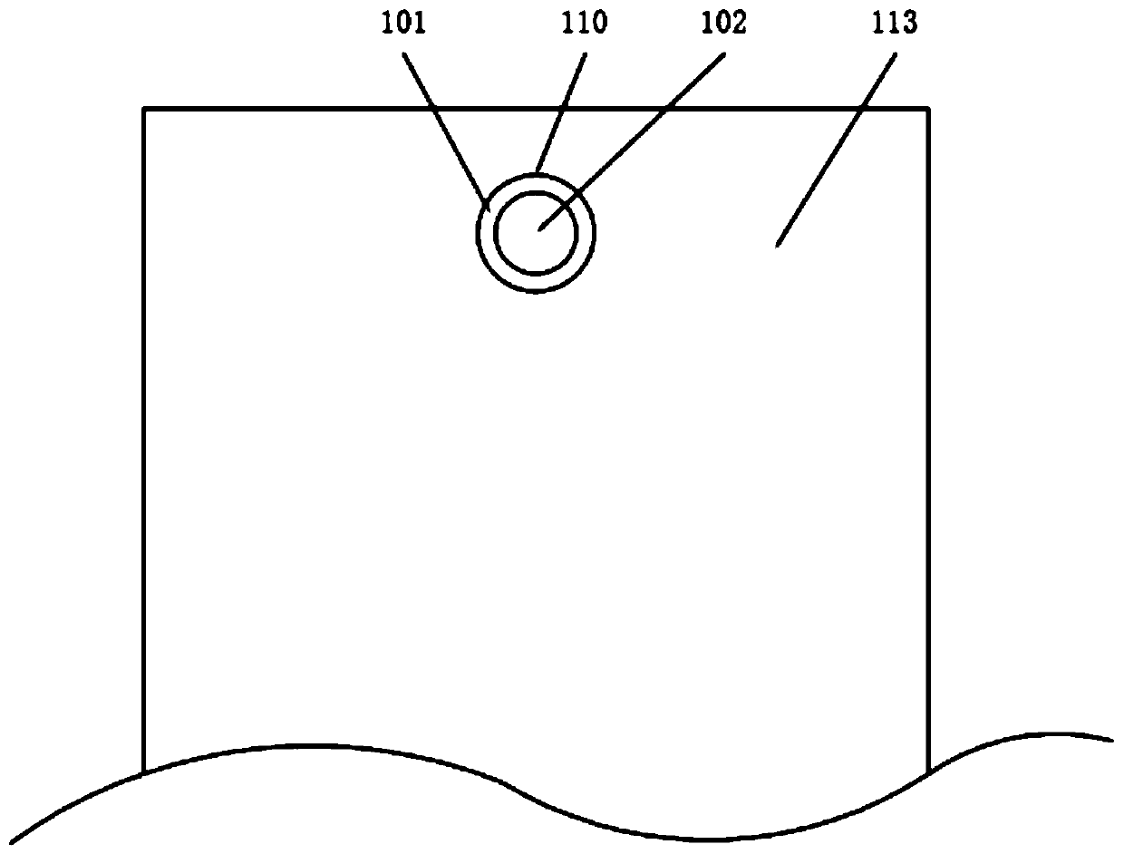
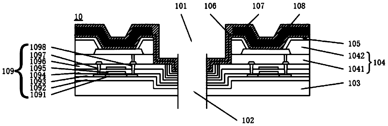
[0038] Such as Figure 1a , 1b As shown, they are schematic plan and cross-sectional diagrams of the ...


PUM


Abstract

The invention discloses an OLED display panel and a manufacturing method thereof. A through hole is formed in the OLED display panel; the through hole comprises a first hole cavity and a second hole cavity; the first hole cavity cuts off a part of a membrane layer exposed by a side wall of the through hole to block a path for water vapor to invade the OLED display panel from the side wall of the through hole; and the second hole cavity penetrates through a substrate, so that clear imaging of a camera at the lower part of a screen is ensured. The OLED display panel has the beneficial effects that part of the membrane layer around the through hole is cut off to cut off a water vapor invasion channel on the side surface of the through hole, so that the packaging reliability of an OLED deviceis guaranteed, the light transmittance of the through hole is improved, and the clear imaging of the camera at the lower part of the screen is guaranteed.

Description

technical field [0001] The invention relates to the field of display technology, in particular to an OLED display panel and a manufacturing method thereof. Background technique [0002] At present, there is a new type of O-cut (O-cut) OLED display panel, which is characterized in that an O-shaped hole is designed in its non-edge display area, and modules such as cameras, infrared sensors, and earpieces can be placed under the O-shaped hole. Since the position of this O-shaped hole can be set at will, it can realize the flexibility of the position of modules such as CUP (under-display camera), infrared sensor, earpiece, etc. in the panel display area. However, due to the many film layers in the OLED panel, the loss of external light after passing through the O-cut area is relatively large, which eventually leads to the inability of the CUP to image clearly. Therefore, how to improve the light transmittance of the O-cut region has become a necessary and practical research pro...

Claims


Application Information

Patent Timeline
Patent Type & Authority Applications(China)
IPC IPC(8): H01L51/52H01L27/32
CPCH10K59/12H10K50/844H10K59/1201Y02E10/549H10K59/122H10K59/124H10K77/10H10K50/80H10K59/65H10K71/00
Inventor 孙佳佳
Owner WUHAN CHINA STAR OPTOELECTRONICS SEMICON DISPLAY TECH CO LTD
Why Eureka
Try Eureka