A kind of composite circuit board and preparation method thereof

A composite circuit and circuit board technology, used in printed circuit manufacturing, printed circuits, printed circuits, etc., can solve problems such as safety hazards, pins that are easy to scratch fingers, and components that are easily damaged.

Active Publication Date: 2021-08-13
惠州市盈帆实业有限公司
View PDF9 Cites 0 Cited by
  • Summary
  • Abstract
  • Description
  • Claims
  • Application Information

AI Technical Summary

Problems solved by technology

[0005] When performing circuit board welding experiments in the laboratory, the pins of the components are generally inserted into the sockets of the circuit board, and then the pins are bent to fix the components on the circuit board. Straighten and pull out the components, but the pins of the components are usually small and sharp. Pulling the pins is easy to scratch your fingers, which has certain safety hazards, and repeatedly pulling the pins is easy to damage the components, and wastes time and experiments. In addition, during the electric welding process, the molten tin may seep from the gap of the socket to the components on the other side of the circuit board, and the high temperature molten tin may easily damage the components

Method used


Image

  • A kind of composite circuit board and preparation method thereof
  • A kind of composite circuit board and preparation method thereof
  • A kind of composite circuit board and preparation method thereof

Examples


Embodiment 1

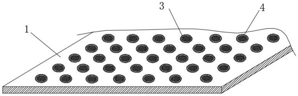
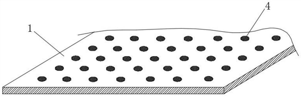
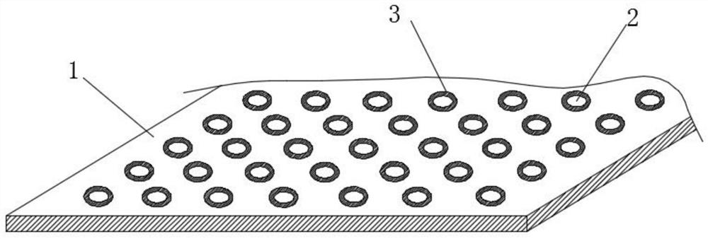
[0047] see image 3 , a composite circuit board, comprising a circuit board body 1, a plurality of jacks 2 are uniformly arranged on the circuit board body 1, a plurality of copper sheets 3 are connected to one end surface of the circuit board body 1, and the plurality of copper sheets 3 are connected to a plurality of Jack 2 matches, see figure 1 , the inner wall of jack 2 is connected with anti-reverse layer 4, please refer to Figure 5 and Figure 6 , the anti-reverse layer 4 includes a first anti-reverse layer 7 and a second anti-reverse layer 6, and the first anti-reverse layer 7 is located on the side of the socket 2 close to the copper sheet 3, and the second anti-reverse layer 6 is located on the side away from the socket 2 On one side of the copper sheet 3, set the socket 2 of the circuit board as a non-return type, so that the molten tin is not easy to seep out from the gap of the socket 2 and damage the components. When inserting components, only the pins of the c...


PUM


Abstract

The invention discloses a composite circuit board and a preparation method thereof, belonging to the field of circuit boards. A composite circuit board includes a circuit board body, a plurality of jacks are uniformly arranged on the circuit board body, and one end surface of the circuit board body is connected with multiple sockets. A copper sheet, and a plurality of copper sheets are matched with a plurality of sockets, the inner wall of the socket is connected with a reverse flow prevention layer, and the reverse flow prevention layer includes a first reverse flow prevention layer and a second reverse flow prevention layer, and the first reverse flow prevention layer is located at The socket is close to the side of the copper sheet, the second anti-reverse layer is located on the side of the socket away from the copper sheet, the first anti-reverse layer includes a plurality of tin strips, and the plurality of tin strips are evenly connected on the inner wall of the socket, and the The socket of the circuit board is set as a non-return type. The molten tin is not easy to seep out from the gap of the socket and damage the components. When inserting components, you only need to insert the pins of the components into the sockets of the circuit board. The reverse jack can automatically fix the components, and when there is an error, it can be pulled out directly, which is safe and convenient.

Description

technical field [0001] The invention relates to the field of circuit boards, and more specifically relates to a composite circuit board and a preparation method thereof. Background technique [0002] The composite structure of the product substrate of the traditional double-sided rigid-flex circuit board is a single-sided rigid board plus a layer of single-sided soft board bonded together by an adhesive. [0003] Main production process: 1. The single-sided PCB substrate is slotted in a specific area first; (the purpose of pre-grooving is to facilitate the removal of the PCB here in the final stage of the product); 2. AD glue is cut in a specific area 3. Paste the PI reinforcement board on a specific area on the single-sided FPC substrate; 4. Use AD glue as the adhesive in the middle layer, and connect the single-sided FPC substrate and the single-sided PCB substrate with The pressing method is combined into one body, and the PI reinforcing plate is also included in it at t...

Claims


Application Information

Patent Timeline
Patent Type & Authority Patents(China)
IPC IPC(8): H05K1/11H05K1/18H05K3/34
CPCH05K1/116H05K1/184H05K3/3447H05K2201/09645
Inventor 李争军刘立冬李爱明
Owner 惠州市盈帆实业有限公司
Why Eureka
Try Eureka