

Display substrate and preparation method thereof, and display device
A technology for display substrates and flexible substrates, used in semiconductor/solid-state device manufacturing, semiconductor devices, electrical components, etc., can solve problems such as luminous instability, and achieve the effects of ensuring luminous stability, improving deformation resistance, and improving display quality.
- Summary
- Abstract
- Description
- Claims
- Application Information
AI Technical Summary
Problems solved by technology
Method used
Image

Examples
no. 1 example
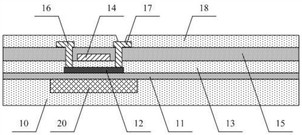
[0051] figure 1 A schematic structural diagram of a substrate is shown for an embodiment of the present invention. Such as figure 1 As shown, the main structure of the display substrate in this embodiment includes a flexible substrate 10, a buffer layer 11 disposed on the flexible substrate 10, and an array structure layer disposed on the buffer layer 11, the array structure layer includes a plurality of thin film transistors, figure 1 Only one thin film transistor is illustrated. Wherein, the thin film transistor includes an active layer 12 , a gate electrode 14 , a source electrode 16 and a drain electrode 17 . In this embodiment, the substrate further includes a reinforcement layer 20 , which is embedded in the flexible substrate 10 in a plane perpendicular to the flexible substrate 10 , and the surface of the reinforcement layer 20 is flush with the surface of the flexible substrate 10 . In a plane parallel to the flexible substrate 10, the position of the reinforcement...
no. 2 example
[0077] Based on the technical concept of the present invention, the embodiment of the present invention also provides a method for preparing a display substrate. The embodiment of the present invention shows that the preparation method of the substrate includes:
[0078] S1, forming a flexible substrate embedded with a strengthening layer;
[0079] S2. Forming a thin film transistor on the flexible substrate, so that the position of the strengthening layer corresponds to the position of the channel region of the thin film transistor, so as to improve the deformation resistance of the channel region of the thin film transistor.
[0080] Wherein, step S1 includes:
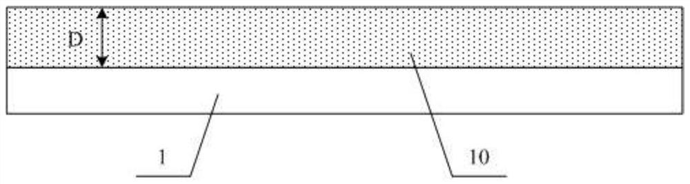
[0081] S11, forming an incompletely cross-linked flexible film on the glass carrier;
[0082] S12. Opening grooves on the incompletely crosslinked flexible film, the depth of the grooves being 30% to 50% of the thickness of the incompletely crosslinked flexible film;
[0083] S13, forming an incompletely crosslink...
no. 3 example
[0095] An embodiment of the present invention also provides a display device, which includes the display substrate of the foregoing embodiment. The display device can be any product or component with a display function such as a mobile phone, a tablet computer, a television, a monitor, a notebook computer, a digital photo frame, a navigator, and the like.
PUM
| Property | Measurement | Unit |
|---|---|---|
| quality score | aaaaa | aaaaa |
Abstract
Description
Claims
Application Information