Polycrystalline silicon wafer solidification device

A technology of polycrystalline silicon wafers and racks, which is applied in spraying devices, devices for coating liquid on the surface, spray booths, etc., can solve problems such as low efficiency, slow film formation speed of polycrystalline silicon wafers, inconvenient polycrystalline silicon wafer solidification operation, etc., to achieve The effect of improving efficiency

Active Publication Date: 2019-10-11
台州锐祥机械设备有限公司
View PDF9 Cites 2 Cited by
  • Summary
  • Abstract
  • Description
  • Claims
  • Application Information

AI Technical Summary

Problems solved by technology

The existing electron beam curing device is inconvenient to solidify polysilicon wafers, and the speed of film formation on polysilicon wafers is slow and the efficiency is low

Method used


Image

  • Polycrystalline silicon wafer solidification device
  • Polycrystalline silicon wafer solidification device
  • Polycrystalline silicon wafer solidification device

Examples


Embodiment Construction

[0020] The preferred embodiments of the present invention will be described in detail below in conjunction with the accompanying drawings, so that the advantages and features of the present invention can be more easily understood by those skilled in the art, so as to define the protection scope of the present invention more clearly.

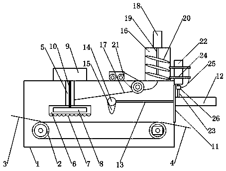
[0021] Such as Figure 1 to Figure 4 As shown, the solidification device for polycrystalline silicon wafers includes a solidification frame 1, the bottom of the solidification frame 1 is provided with a belt conveyor 2, one side of the solidification frame 1 is provided with a feeding table 3, and the other side of the solidification frame 1 is provided with There is a discharge table 4, the feed table 3 is connected to one side of the belt conveyor 2, and the discharge table 4 is connected to the other side of the belt conveyor 2; the inner top of the solidification frame 1 is provided with a ceiling pipe 5, and the ceiling pipe The lower end of...


PUM


Abstract

The invention discloses a polycrystalline silicon wafer solidification device. The polycrystalline silicon wafer solidification device comprises a solidification rack, wherein a belt conveyor is arranged at the lower part of the solidification rack; a feeding platform is arranged at one side of the solidification rack; a discharging platform is arranged at the other side of the solidification rack; the feeding platform is connected to one side of the belt conveyor; the discharging platform is connected to the other side of the belt conveyor; a suspended ceiling pipe is arranged on the inner top of the solidification rack; a pasty polyvinyl chloride resin liquid spraying bin is arranged at the lower end of the suspended ceiling pipe; a plurality of pasty polyvinyl chloride resin liquid spraying nozzles are arranged on the bottom surface of the pasty polyvinyl chloride resin liquid spraying bin and are located above the belt conveyor; a spraying machine is arranged on the top of the solidification rack; a spraying inner pipe is arranged inside the suspended ceiling pipe; the upper end of the spraying inner pipe is connected to the spraying machine; and the lower end of the spraying inner pipe communicates with the pasty polyvinyl chloride resin liquid spraying bin. The polycrystalline silicon wafer solidification device greatly improves the efficiency of solidification treatmentand enables pasty polyvinyl chloride resin liquid to quickly form a film on the surface of a polycrystalline silicon wafer.

Description

technical field [0001] The invention relates to a solidification device, in particular to a solidification device for a polycrystalline silicon wafer. Background technique [0002] The electron beam curing device is characterized by fast curing speed and small heat transfer to the object to be irradiated. It is especially suitable for pressure-sensitive adhesive products and other composite products of paper base, film, foam and metal box piano. It can be divided into high-energy type, Simple energy type and low energy type heart. Polycrystalline silicon wafer is a form of elemental silicon. When molten elemental silicon is solidified under supercooled conditions, silicon atoms are arranged in the form of diamond lattices to form many crystal nuclei. If these crystal nuclei grow into crystal grains with different crystal plane orientations, these crystal grains combine to crystallize into polycrystalline silicon. . The existing electron beam solidification device is incon...

Claims


Application Information

Patent Timeline
Patent Type & Authority Applications(China)
IPC IPC(8): B05B16/20B05B15/25B05B13/02B05D3/14
CPCB05B13/0221B05D3/14B05B15/25B05B16/20
Inventor 不公告发明人
Owner 台州锐祥机械设备有限公司
Why Eureka
Try Eureka