Method and device for predicting surface morphology after CMP

A surface topography and prediction method technology, which is applied in the field of surface topography prediction after CMP, can solve problems such as prediction deviation and difficult application of post-surface topography prediction

Active Publication Date: 2019-10-11
INST OF MICROELECTRONICS CHINESE ACAD OF SCI
View PDF5 Cites 0 Cited by
  • Summary
  • Abstract
  • Description
  • Claims
  • Application Information

AI Technical Summary

Problems solved by technology

When using the current post-CMP surface topography prediction method to predict the planarized topography of small-sized device wafers, there

Method used


Image

  • Method and device for predicting surface morphology after CMP
  • Method and device for predicting surface morphology after CMP
  • Method and device for predicting surface morphology after CMP

Examples


Embodiment Construction

[0038] In order to make the above objects, features and advantages of the present invention more comprehensible, specific implementations of the present invention will be described in detail below in conjunction with the accompanying drawings.

[0039] In the following description, a lot of specific details are set forth in order to fully understand the present invention, but the present invention can also be implemented in other ways different from those described here, and those skilled in the art can do it without departing from the meaning of the present invention. By analogy, the present invention is therefore not limited to the specific examples disclosed below.

[0040] As described in the background technology, with the continuous shrinking of the feature size of the device, after the manufacturing process enters the process node below 28 nanometers, using the current post-CMP surface topography prediction method, the flattened topography of the crystal element of the s...


PUM


Abstract

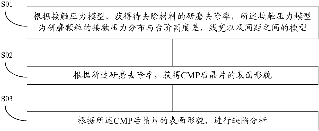
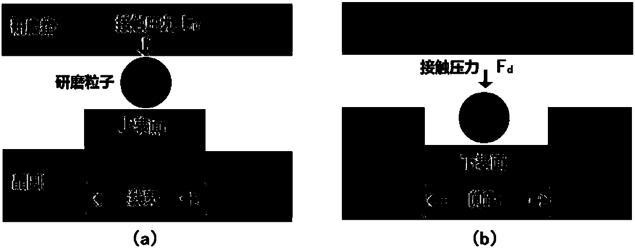
The invention provides a method and a device for predicting surface morphology after CMP (Chemical Mechanical Planarization). When a grinding removal rate of a material to be removed is obtained, a contact pressure model is adopted as a numerical model between the contact pressure distribution of grinding particles and the step height difference, the line width and the space, and the influence ofthe grinding particles on the removal rate of the material to be removed is fully considered, so that the actual process condition of CMP can be described more objectively and truly, more accurate surface morphology prediction and defect prediction after CMP can be achieved, the precision of surface morphology prediction after CMP is improved, the method and the device are particularly suitable for the surface morphology prediction after CMP of small-size device wafers, and guidance is provided for parameter setting and design optimization in a CMP process.

Description

technical field [0001] The invention relates to the technical field of integrated circuit simulation modeling, in particular to a method and device for predicting surface topography after CMP. Background technique [0002] Chemical Mechanical Planarization (CMP) is an important part of fine surface processing in semiconductor manufacturing technology, and has become the most widely used planarization technology in the era of very large scale integrated circuits. , so that the grinding surface reaches a nano-level smoothness. [0003] With the continuous shrinking of the feature size of the device, after the manufacturing process enters the process node below the 28nm level, the problem of the flatness of the wafer has become increasingly prominent, and the process fault tolerance has also been reduced to the nanometer level. By predicting the topography of the chip surface after CMP, the reading changes on the surface of the polished wafer can be obtained, and the real-time...

Claims


Application Information

Patent Timeline
IPC IPC(8): H01L21/66H01L21/306G01R31/26
CPCG01R31/2601H01L21/30625H01L22/12
Inventor 曹鹤陈岚孙艳张贺彩虹
Owner INST OF MICROELECTRONICS CHINESE ACAD OF SCI
Why Eureka
Try Eureka