Silica-based micro display screen and preparation method thereof

A display, silicon-based technology, used in semiconductor/solid-state device manufacturing, electrical components, electrical solid-state devices, etc., can solve problems such as physical bottlenecks in manufacturing technology, and achieve the effect of preventing optical crosstalk and high pixel density

Pending Publication Date: 2019-10-11
KUNSHAN FANTAVIEW ELECTRONICS TECH CO LTD
0 Cites 1 Cited by

AI-Extracted Technical Summary

Problems solved by technology

[0002] Most of the current OLED display body uses evaporation of different OLED materials to achieve OLED patterning. This method is no problem when the ...

Abstract

The invention provides a silica-based micro display screen and a preparation method thereof. The silica-based micro display screen comprises a driving backboard, a pixel definition layer formed on thedriving backboard, a light emitting layer formed in the pixel definition layer, a packaging layer for packaging the light emitting layer, and a metal reflection layer formed between the light emitting layer and the packaging layer. Compared with the prior art, the silica-based micro display screen breaks through the physical limit of high-precision metal masks with high pixel density, and is capable of realizing the display with 2000 and higher pixel density.

Application Domain

Solid-state devicesSemiconductor/solid-state device manufacturing +1

Technology Topic

Pixel densityBackplane +2

Image

  • Silica-based micro display screen and preparation method thereof
  • Silica-based micro display screen and preparation method thereof
  • Silica-based micro display screen and preparation method thereof

Examples

  • Experimental program(1)

Example Embodiment

[0030] In order to make the purpose, technical solutions and effects of this application clearer and clearer, the following further describes this application in detail with reference to the drawings and embodiments.
[0031] The present invention provides a silicon-based micro display screen and a preparation method thereof, which are mainly used to solve the problems of the physical limitation of the existing OLED evaporation patterning technology and the difficulty of high pixel density patterning.
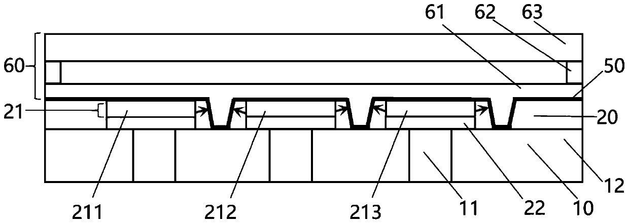
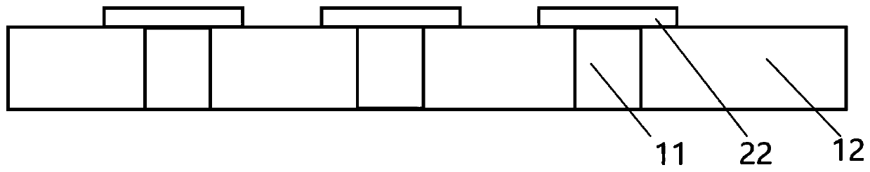
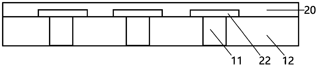
[0032] Such as figure 1 As shown, the silicon-based micro display screen includes: a driving backplane 10, a pixel definition layer 20 formed on the driving backplane 10, a light-emitting layer 21 formed in the pixel definition layer 20, and a encapsulation device. The encapsulation layer 60 of the light-emitting layer 21 and the metal reflective layer 50 formed between the light-emitting layer 21 and the encapsulation layer 60.
[0033] The driving backplane 10 includes a silicon substrate 12 and an anode layer 22 formed on one side of the silicon substrate 12. The light-emitting layer 21 is formed in the pixel defining layer 20 by electrofluid printing and is located on the anode. Above layer 22.
[0034] Specifically, the silicon substrate 12 is provided with a plurality of regularly arranged vias 11, the anode layer 22 includes a plurality of anode units arranged in a pixel pattern, and each anode unit is connected to the corresponding via 11 one by one. Correspondingly, the anode unit is an indium tin oxide film (ITO). In this embodiment, the width of the anode unit is 5 microns, but it should not be limited to this.
[0035] The pixel definition layer 20 is formed by a yellow light process and an etching process, and the anode layer 22 is exposed to the pixel definition layer 20. Preferably, the pixel definition layer 20 is made of SiO 2 The photolithography mask is a material, and a film is formed on the silicon substrate 12 and the anode layer 22.
[0036] The light emitting layer 21 includes an organic light emitting layer, a hole injection layer and a hole transport layer located between the anode layer 22 and the organic light emitting layer, and an electron injection layer and an electron transport layer located between the cathode layer and the organic light emitting layer. Further, the hole transport layer is located between the organic light emitting layer and the hole injection layer; the electron transport layer is located between the organic light emitting layer and the electron injection layer.
[0037] The light-emitting layer 21 includes sub-pixels spaced apart from each other. The sub-pixels include a first sub-pixel 211, a second sub-pixel 212, and a third sub-pixel 213, and the distance between two adjacent sub-pixels is 8 microns. Specifically, the first sub-pixel 211 is an OLED that can emit red light R, the second sub-pixel 212 is an OLED that can emit green light G, and the third sub-pixel 213 is an OLED that can emit blue light B. Thus, RGB three-color display can be realized.
[0038] The metal reflective layer 50 is formed on the upper surface of the light-emitting layer 21 and the pixel definition layer 20, and the metal reflective layer 50 is also formed between two adjacent sub-pixels, so as to avoid the interference between the two adjacent sub-pixels. Optical crosstalk. In the present invention, the metal reflective layer 50 is an Al reflective layer and can be used as the cathode layer of the light-emitting layer 21.
[0039] The packaging layer 60 includes a thin film packaging layer 61, and the thin film packaging layer 61 completely covers the metal reflective layer 50. The packaging layer 60 also includes a glass cover plate 63 encapsulated on the top of the thin film packaging layer 61 and completely covering the thin film packaging layer 61. Specifically, the glass cover plate 63 is fixedly connected to the thin film encapsulation layer 61 through UV glue 62.
[0040] The thin film encapsulation layer 61 may be an organic thin film, an inorganic thin film, or an inorganic thin film stacked on an organic thin film.
[0041] Such as Figure 1 to Figure 6 As shown, the manufacturing method of silicon-based microdisplay mainly includes the following steps:
[0042] S1: A silicon substrate 12 is provided, and an anode layer 22 is vapor-deposited on the silicon substrate 12 to form the driving backplane 10; at this time, each anode unit of the anode layer 22 is connected to the corresponding via 11 one by one Corresponding, specifically as figure 2 Shown.
[0043] S2: Plating a film on the silicon substrate 12 and the anode layer 22 to form a pixel definition layer 20; at this time, the pixel definition layer 20 completely covers the silicon substrate 12 and the anode layer 22, specifically as follows image 3 Shown.
[0044] S3: Use yellow light process and etching process to etch the pixel defining layer 20; after the etching, the anode layer 22 is exposed to the pixel defining layer 20, specifically as Figure 4 Shown.
[0045] S4: Using electrofluidic printing technology, a light-emitting layer 21 is formed in the pixel defining layer 20; at this time, the light-emitting layer 21 is formed on the anode layer 22, and the first sub-pixel 211 and the second sub-pixel 212 And the third sub-pixel 213 are respectively formed on the corresponding anode unit, specifically as Figure 5 Shown.
[0046] S5: forming a metal reflective layer 50 on the light emitting layer 21 and the pixel defining layer 20; at this time, the metal reflective layer 50 is not only formed on the light emitting layer 21 and the pixel defining layer 20, but also formed between two adjacent sub-pixels For example, formed between the first sub-pixel 211 and the second sub-pixel 212, and between the second sub-pixel 212 and the third sub-pixel 213, specifically as Image 6 Shown.
[0047] S6: Encapsulate the metal reflective layer 50 to obtain a silicon-based micro display screen; figure 1 Shown.
[0048] The step S6 specifically includes:
[0049] S61: Using thin film packaging technology to form a thin film packaging layer 61 on the metal reflective layer 50;
[0050] S62: Use a glass cover plate 63 to encapsulate the thin-film packaging layer 61, and use UV glue 62 to fix the thin-film packaging layer 61 above the thin-film packaging layer 61.
[0051] In summary, the present invention ① uses the high-resolution drive backplane 10 to realize the preparation of high-resolution display screens of 1000 ppi and above; ② realizes high-ppi micro-display graphics through yellow light process and etching process , Breaking through the physical limit of high-pixel-density high-precision metal masks, can achieve 2000 and higher pixel density display, and in the use of raw materials, it saves about 90% compared with evaporation technology; ③printing by electrofluid Technology printing small-size RGB three-color OLED can realize the RGB three-color display of silicon-based micro-display; ④The metal reflective layer 50 is formed between the light-emitting layer 21 and the encapsulation layer 60, which can prevent two adjacent sub-pixels Light crosstalk occurs between.
[0052] The above are only specific embodiments of the present invention, but the protection scope of the present invention is not limited to this. Anyone familiar with the technology can understand the changes or substitutions that are conceivable within the technical scope disclosed in the present invention. All should be covered within the scope of the present invention. Therefore, the protection scope of the present invention should be subject to the protection scope of the claims.

PUM

no PUM

Description & Claims & Application Information

We can also present the details of the Description, Claims and Application information to help users get a comprehensive understanding of the technical details of the patent, such as background art, summary of invention, brief description of drawings, description of embodiments, and other original content. On the other hand, users can also determine the specific scope of protection of the technology through the list of claims; as well as understand the changes in the life cycle of the technology with the presentation of the patent timeline. Login to view more.

Similar technology patents

TFT array substrate manufacture method

ActiveCN105702623Areduce sizeincrease pixel density
Owner:WUHAN CHINA STAR OPTOELECTRONICS TECH CO LTD

Sound wave phase modulation and sound field reconstruction method based on near-field orbital angular momentum conversion

ActiveCN114543980Asmall geometryIncrease Pixel Density
Owner:BEIJING INSTITUTE OF TECHNOLOGYGY

Solid-state image pickup device

InactiveUS6933976B1increase pixel density
Owner:FUJIFILM CORP

OLED display substrate, manufacturing method thereof and display device

ActiveCN110993834Aincrease pixel density
Owner:BOE TECH GRP CO LTD

Integrated Micro LED chip and manufacturing method thereof

ActiveCN113270440Aavoid optical crosstalkreduce complexity
Owner:FUJIAN PRIMA OPTOELECTRONICS CO LTD

Classification and recommendation of technical efficacy words

  • avoid optical crosstalk
  • increase pixel density

Integrated Micro LED chip and manufacturing method thereof

ActiveCN113270440Aavoid optical crosstalkreduce complexity
Owner:FUJIAN PRIMA OPTOELECTRONICS CO LTD

Solid-state image pickup device

InactiveUS6933976B1increase pixel density
Owner:FUJIFILM CORP

TFT array substrate manufacture method

ActiveCN105702623Areduce sizeincrease pixel density
Owner:WUHAN CHINA STAR OPTOELECTRONICS TECH CO LTD

OLED display substrate, manufacturing method thereof and display device

ActiveCN110993834Aincrease pixel density
Owner:BOE TECH GRP CO LTD

Sound wave phase modulation and sound field reconstruction method based on near-field orbital angular momentum conversion

ActiveCN114543980Asmall geometryIncrease Pixel Density
Owner:BEIJING INSTITUTE OF TECHNOLOGYGY
Why Eureka
Try Eureka