

Image display element
An image display and component technology, applied in optical components, electrical components, electrical solid-state devices, etc., to achieve the effects of low power consumption, prevention of optical crosstalk, and high color purity
- Summary
- Abstract
- Description
- Claims
- Application Information
AI Technical Summary
Problems solved by technology
Method used
Image

Examples
no. 1 approach 〕
[Configuration of Image Display Device 200 ]
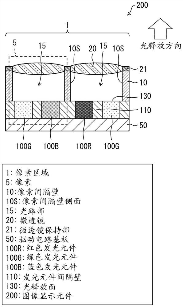
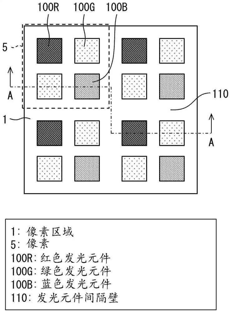
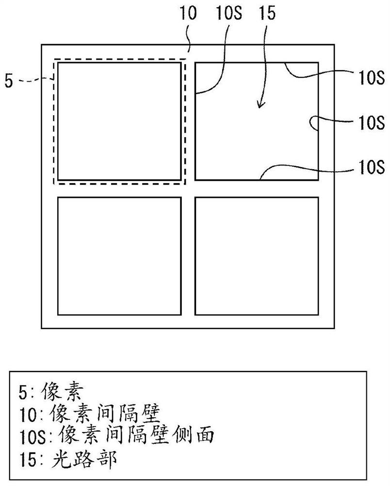
figure 1 It is a schematic cross-sectional view of the pixel region 1 of the image display element 200 according to the first embodiment of the present invention. figure 2 This is a schematic plan view of the light emission surface 130 of the micro light-emitting element 100 according to the first embodiment of the present invention. like figure 2 As shown, there is a pixel region 1 in which a plurality of pixels 5 are arranged in an array on the upper surface of the image display element 200 .
[0032] In the present embodiment, the image display element 200 is a full-color display element, and each pixel 5 includes one blue light-emitting element 100B, two green light-emitting elements 100G, and one red light-emitting element 100R. In addition, the blue light emitting element 100B, the green light emitting element 100G, and the red light emitting element 100R are collectively referred to as the micro light emitting el...
no. 2 approach 〕
use Figure 5 The second embodiment will be described. In the first embodiment, both surfaces of the microlens 20 are convex. In the image display element 200a of the present embodiment, the microlens 20a has a convex shape on the side of the microlight emitting element 100, but the surface on the side in the light emission direction is flat. Other than that, there is no change from the first embodiment.
[0051] In the image display element 200a, the microlens holding portion 21a can be easily thickened, and the mechanical strength of the microlens array can be increased. As a result, the fabrication of the microlens array can be separated from the microlight emitting element 100 . For example, a glass substrate can be used as the microlens holding portion 21a, and after forming the convex-shaped microlenses 20a thereon, it can be attached to the micro light-emitting element 100 via the pixel partition walls 10. Thereby, the production efficiency of the image display el...
no. 3 approach 〕
use Image 6 A third embodiment will be described. In the first embodiment, the optical path portion 15 serving as the space between the microlens 20 and the microlight emitting element 100 is a space filled with gas, but in the image display element 200b of the present embodiment, the same as that described in the first embodiment The part corresponding to the optical path part 15 of the 10 is replaced by the transparent part 11 . In this way, the optical path portion 15 surrounded by the micro light-emitting element 100 , the pixel partition walls 10 and the microlenses 20b is filled with the transparent material.
[0055] In addition, the microlens 20b has a convex shape in the light emission direction, but the surface on the side of the microlight emitting element 100 is flat. Other than that, there is no change from the first embodiment. In addition, the side which is in contact with the transparent portion 11 of the microlens 20b may have a downward convex shape. ...
PUM
 Abstract
Description
Claims
Application Information