Pixel structure of cmos image sensor and its manufacturing method

A technology of image sensor and pixel structure, applied in the direction of radiation control devices, etc., can solve problems such as sensitivity, resolution and definition deterioration, pixel optical crosstalk, chip performance deterioration, etc., to improve optical resolution and sensitivity , Improve light absorption, improve performance and reliability

Active Publication Date: 2018-10-16
SHANGHAI INTEGRATED CIRCUIT RES & DEV CENT
View PDF6 Cites 0 Cited by
  • Summary
  • Abstract
  • Description
  • Claims
  • Application Information

AI Technical Summary

Problems solved by technology

However, the light transmission of conventional semiconductor materials is poor, so it is necessary to remove all the dielectric layer above the photosensitive element and fill it with a light-transmitting material to enhance its light absorption.
[0004] However, as the pixel size decreases, the distance between adjacent pixels also decreases sharply. When light is incident, the light will pass through the area between adjacent pixels through refraction and multiple reflections to reach the side One pixel, which will cause optical crosstalk between pixels, resulting in poor image signal sensitivity, resolution and clarity of the pixel, and poor chip performance

Method used


Image

  • Pixel structure of cmos image sensor and its manufacturing method
  • Pixel structure of cmos image sensor and its manufacturing method
  • Pixel structure of cmos image sensor and its manufacturing method

Examples


no. 1 example

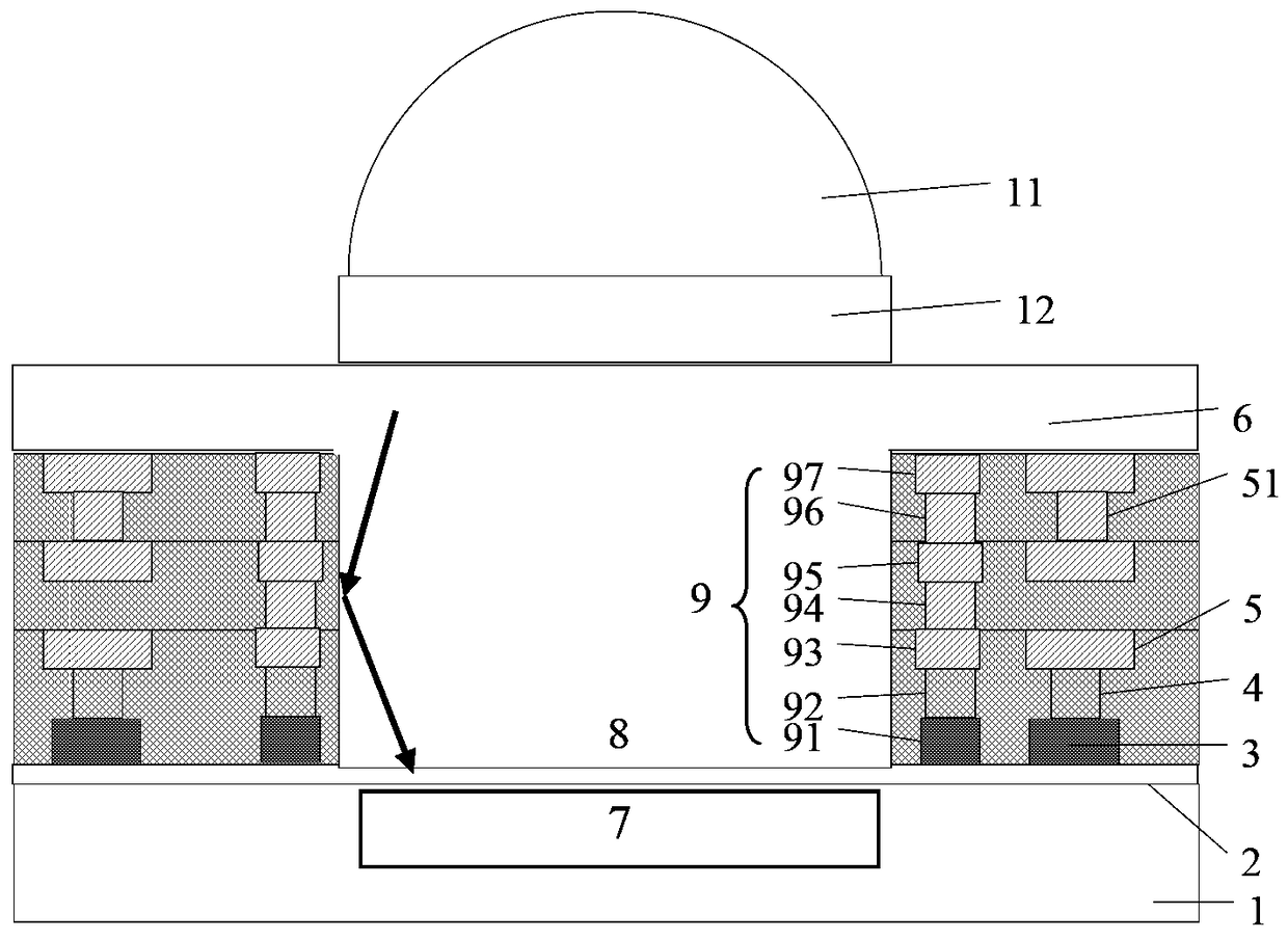
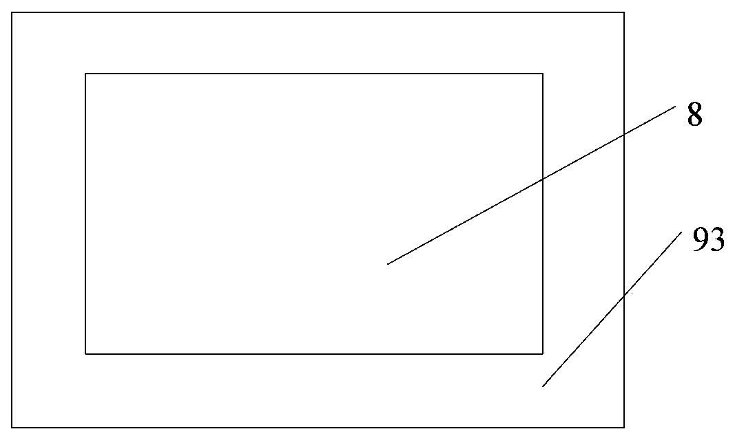
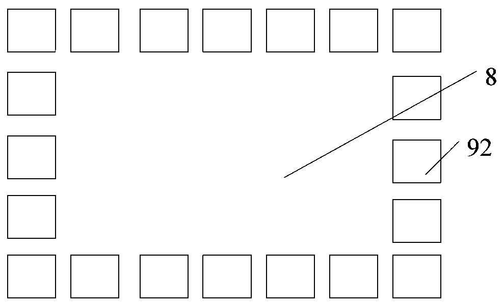
[0041] see figure 1 , the pixel structure of the CMOS image sensor includes a photodiode 7 and a multilayer structure (for standard CMOS devices) on the silicon substrate 1, and there is also a layer between the silicon substrate 1 and the multilayer structure in this embodiment Gate oxide layer 2, wherein the multi-layer structure includes from bottom to top the first polysilicon layer 3, the W contact hole layer 4, the Cu metal interconnection layer 5 and the first via hole layer 51, the interconnection dielectric layer (not marked), a deep groove 8 is arranged above the photodiode 7, and a light reflection shielding layer 9 is also provided in the side wall medium of the deep groove 8, and the distance between the light reflection shielding layer 9 and the side wall of the deep groove 8 is 0.1um , it completely surrounds the deep trench 9, and it includes a second polysilicon layer 91, a second contact hole layer 92, and a second metal interconnection layer A that are conti...

no. 2 example

[0052] In this embodiment, the light reflection shielding layer is a metal layer surrounded by metal, and is arranged vertically from the grid oxide layer upwards continuously to form a whole.

[0053] see Figure 4a to Figure 4d , the manufacturing method of the pixel structure of the CMOS image sensor of the present embodiment comprises the following steps:

[0054] Step S101: arranging photodiodes and multilayer structures for standard CMOS devices on a silicon substrate, and utilizing standard CMOS processes to realize photodiodes and multilayer structures;

[0055] Step S102: using a photolithography process to realize the through hole 101 on the top layer of the multilayer structure and the hole groove 102 for accommodating the light reflection shielding layer;

[0056] Step S103: Realize the groove 103 for accommodating metal wiring in the first metal interconnection layer on the top layer of the multilayer structure by using a photolithography process;

[0057] Step ...


PUM


Abstract

The invention discloses a picture element structure of a CMOS (complementary metal oxide semiconductor) image sensor and a manufacturing method thereof. The structure comprises a light-sensitive element on a silicon substrate and a multi-layer structure for a CMOS device, wherein the multi-layer structure comprises a polysilicon layer, a contact hole layer, a metal interconnection layer, a through hole layer and an interconnection medium layer; the space above the light-sensitive element is surrounded by a light reflecting and shielding layer; and the light reflecting and shielding layer comprises a first polysilicon layer, a first contact hole layer and a first metal interconnection layer from bottom to top. The picture element structure disclosed by the invention enables a deep groove to be surrounded by an annular metal interconnection line, a through hole, a contact hole and polysilicon, enables the incident light on the deep groove to be basically completely reflected, avoids the occurrence of optical crosstalk, effectively improves the optical resolution and sensitivity of a picture element, and increases the performance and reliability of a chip.

Description

technical field [0001] The invention relates to the technical field of CMOS image sensors, in particular to a pixel structure of a CMOS image sensor and a manufacturing method thereof. Background technique [0002] The CMOS image sensor has been developed rapidly due to its compatibility with the CMOS process. Compared with the CCD process, its process is completely compatible with the CMOS process. By making the photosensitive element and the CMOS processing circuit together on the silicon substrate, the cost is greatly reduced on the basis of ensuring performance, and the integration level can be greatly improved. , to manufacture products with higher pixels. [0003] The traditional CMOS image sensor uses the method of front lighting, and the photosensitive element and the CMOS processing circuit are implemented together on the silicon substrate at the same level, while the chip interconnection is fabricated on the CMOS processing circuit, and the photosensitive element ...

Claims


Application Information

Patent Timeline
Patent Type & Authority Patents(China)
IPC IPC(8): H01L27/146
Inventor 赵宇航康晓旭顾学强
Owner SHANGHAI INTEGRATED CIRCUIT RES & DEV CENT
Why Eureka
Try Eureka