Solid-state photodetector
A photodetector and solid-state technology, which is applied in the direction of electric solid-state devices, semiconductor devices, televisions, etc., can solve the problem of unstable sensitivity and achieve the effect of suppressing interference
- Summary
- Abstract
- Description
- Claims
- Application Information
AI Technical Summary
Problems solved by technology
Method used
Image


Examples
no. 1 approach
[0056] refer to Figure 1 to Figure 10 The structure of the solid-state photodetector 10 according to the first embodiment of the present invention will be described.
[0057] (Structure of solid-state photodetector)
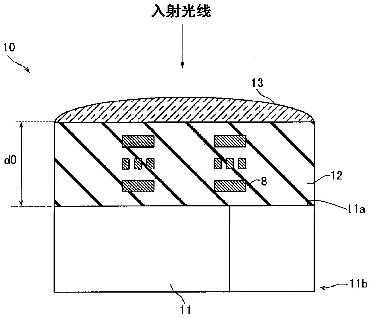
[0058] The solid-state photodetector 10 is composed of, for example, a CMOS (complementary metal oxide semiconductor: complementary metal oxide semiconductor) sensor and a CCD (Charge Coupled Device: charge coupled device) sensor including a light receiving unit 11 (photodiode). In the first embodiment, the solid-state photodetector 10 is a surface incidence type in which light is incident from the side where the wiring pattern 8 is provided.
[0059] Such as figure 1 As shown in FIG. 1 , a surface-incident type solid-state photodetector 10 includes a light-receiving unit 11 . Such as figure 2 As shown, a plurality of light receiving units 11 are provided. The plurality of light receiving units 11 are arranged in a matrix in plan view (when viewed from th...
no. 2 approach
[0087] Next, refer to Figure 11 Next, a second embodiment will be described. In this second embodiment, the functional layer 43 has a cylindrical lens shape.
[0088] Such as Figure 11 As shown, in the solid-state photodetector 40 of the second embodiment, the functional layer 43 has a cylindrical lens shape that gives curvature to the wavefront in a uniaxial direction with respect to a plane wave incident on the functional layer 43 . Specifically, the functional layer 43 has a cylindrical lens shape protruding toward the light-incident side. More specifically, the focal point of the cylindrical lens exists near the light receiving surface 11a. In addition, the functional layer 43 is formed by chiseling or the like on the base layer of the functional layer 43 after forming a base layer (not shown) of the functional layer 43 . In addition, a preformed functional layer 43 may also be bonded to the surface of the surface film 12 .
[0089] In addition, the effects of the s...
no. 3 approach
[0091] Next, refer to Figure 12 A third embodiment will be described. In this third embodiment, the functional layer 93 of one shape (one lens shape) is provided over the plurality of light receiving sections 11 .
[0092] Such as Figure 12 As shown, in the solid-state photodetector 90 of the third embodiment, a single-shaped functional layer 93 is provided so as to cover the plurality of light receiving units 11 arranged in a matrix. Specifically, the functional layer 93 has a substantially circular shape in plan view, and is provided so as to partially cover the plurality of light receiving units 11 arranged in a matrix. In addition, the functional layer 93 has, for example, a convex lens shape. Additionally, it can be done as Figure 12 Like the functional layer 93a indicated by the dotted line, the functional layer 93a is provided so as to cover the entirety of the plurality of light receiving sections 11 arranged in a matrix.
[0093] Alternatively, it could be, fo...
PUM
 Abstract
Description
Claims
Application Information
 - R&D
- Intellectual Property
- Life Sciences
- Materials
- Tech Scout
- Unparalleled Data Quality
- Higher Quality Content
- 60% Fewer Hallucinations
Browse by: Latest US Patents, China's latest patents, Technical Efficacy Thesaurus, Application Domain, Technology Topic, Popular Technical Reports.
© 2025 PatSnap. All rights reserved.Legal|Privacy policy|Modern Slavery Act Transparency Statement|Sitemap|About US| Contact US: help@patsnap.com