LED chip maintenance method and device

A technology for LED chips and chips, which is applied to cleaning methods, chemical instruments and methods, cleaning methods and utensils using gas flow, etc., can solve problems such as chips or first solder residues, and achieve simple removal, low cost, and guaranteed quality. Effect

Inactive Publication Date: 2019-10-25
LEDMAN OPTOELECTRONIC HZ CO LTD +1
View PDF7 Cites 10 Cited by
  • Summary
  • Abstract
  • Description
  • Claims
  • Application Information

AI Technical Summary

Problems solved by technology

[0004] Based on this, it is necessary to provide a maintenance method and a maintenance device for an LED chip for the problem t

Method used


Image

  • LED chip maintenance method and device
  • LED chip maintenance method and device
  • LED chip maintenance method and device

Examples


Embodiment Construction

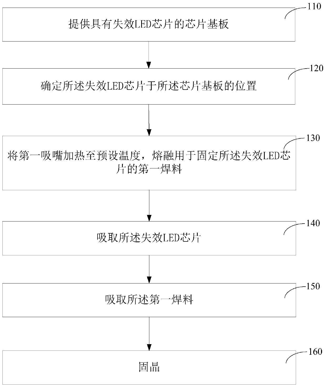
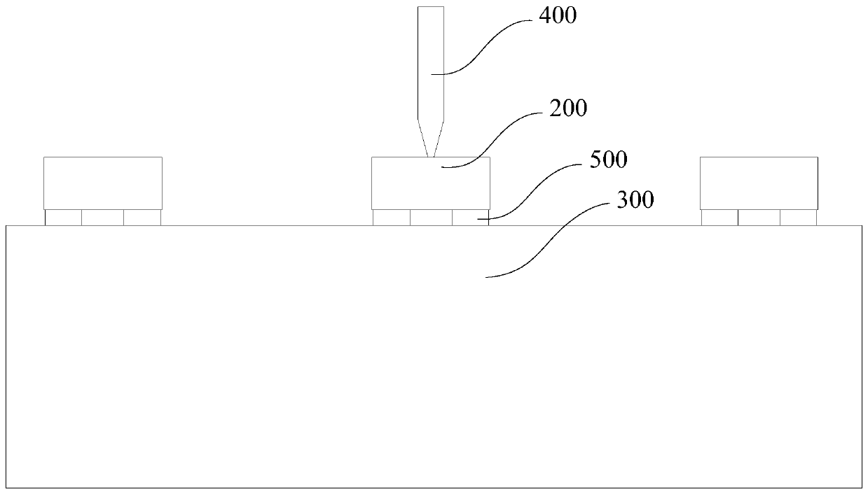
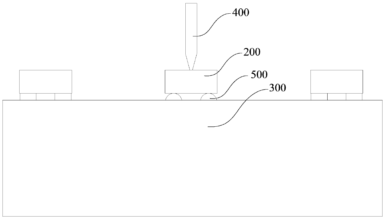
[0034] In order to facilitate the understanding of the present invention, the LED chip maintenance method and maintenance device will be more fully described below with reference to the relevant drawings. The preferred embodiment of the maintenance method and the maintenance device of the LED chip is given in the accompanying drawings. However, the LED chip repair method and repair device can be implemented in many different forms, and are not limited to the embodiments described herein. On the contrary, the purpose of providing these embodiments is to make the disclosure of the LED chip maintenance method and maintenance device more thorough and comprehensive.

[0035] It should be noted that when an element is referred to as being “fixed” to another element, it can be directly on the other element or there can also be an intervening element. When an element is referred to as being "connected to" another element, it can be directly connected to the other element or interveni...


PUM


Abstract

The invention relates to an LED chip maintenance method. The LED chip maintenance method comprises steps that S1, a chip substrate having a failed LED chip is provided; S2, the position of the failedLED chip on the chip substrate is determined; S3, a first nozzle is heated to a preset temperature, and the first solder for fixing the failed LED chip is melted; S4, the failed LED chip is sucked; S5, the first solder is sucked; and S6, die bonding is performed. The method is advantaged in that when the LED chip fails, the first nozzle is heated to fuse the first solder connecting the failed LEDchip with the chip substrate, after the first solder is melted, the failed chip is sucked, the first solder is removed by suction, so elimination of a failure point of the chip substrate is simple, fast, and efficient, professional equipment is not needed, cost is low, moreover, the failed chip and the first solder can be removed, the quality of subsequent die bonding is guaranteed, and the methodis especially suitable for maintenance of small-pitch LED products such as COB flip chips.

Description

technical field [0001] The invention relates to the technical field of LED packaging, in particular to a maintenance method and a maintenance device for an LED chip. Background technique [0002] The existing small-pitch LED display screen can be realized by two methods: lamp bead patch and COB technology. The bad lamp beads detected by SMD packaging do not need to be repaired, but are directly scrapped. Lamp beads that fail the test after the SMT process can also be repaired and replaced, and modules with high failure rates can also be replaced. [0003] Problematic unit boards that fail the test before COB packaging can be repaired by returning to die bonding or returning to bonding wires to achieve a 100% yield rate. The failure point is manually observed, and after remembering the position, use an appropriate thrust to scrape off the traces and then refill the crystal and solder the wire. If there is a failure, use the method of drilling holes to remove the glue, use a...

Claims


Application Information

Patent Timeline
IPC IPC(8): H01L33/62H01L21/67H01L21/683B08B5/04
CPCB08B5/04H01L21/67103H01L21/6838H01L33/62H01L2933/0066
Inventor 李漫铁谢玲屠孟龙余亮俞苗
Owner LEDMAN OPTOELECTRONIC HZ CO LTD
Why Eureka
Try Eureka