

Power semiconductor device
一种功率半导体、元件的技术,应用在半导体器件、电气元件、电路等方向,能够解决高击穿电压困难、功率半导体元件低导通阻抗等问题,达到消除电场扭曲现象、改善击穿电压、良好元件特性的效果
- Summary
- Abstract
- Description
- Claims
- Application Information
AI Technical Summary
Problems solved by technology
Method used
Image

Examples
Embodiment Construction
[0021] The present invention will be described more fully with reference to the accompanying drawings of this embodiment. However, the present invention can also be embodied in various forms and should not be limited to the embodiments described herein. In the drawings, the thicknesses of layers and regions may be exaggerated for clarity. The same or similar symbols represent the same or similar elements, and the following paragraphs will not repeat them one by one.
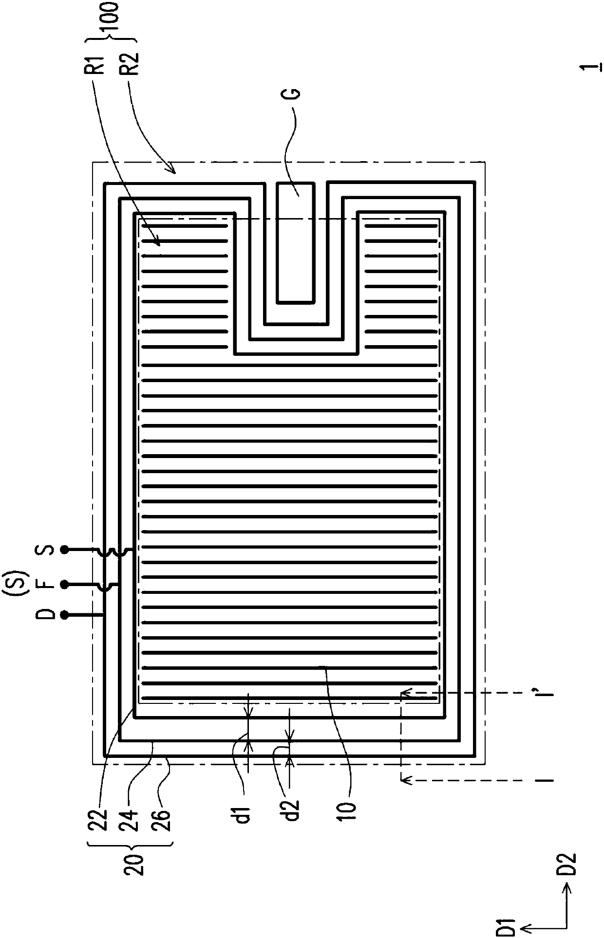
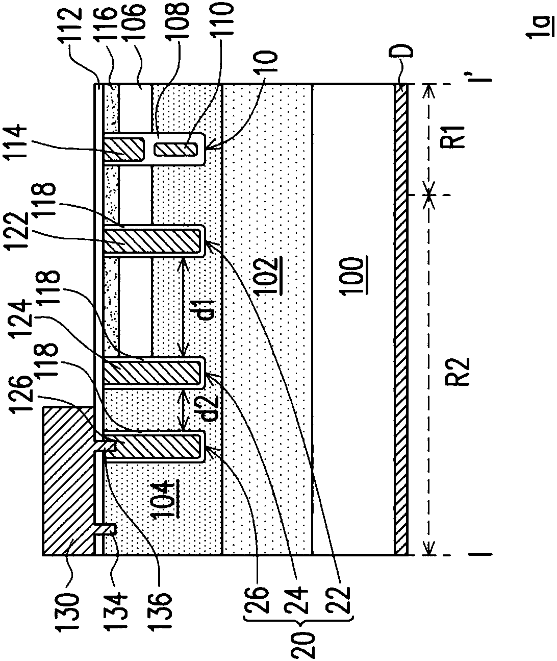
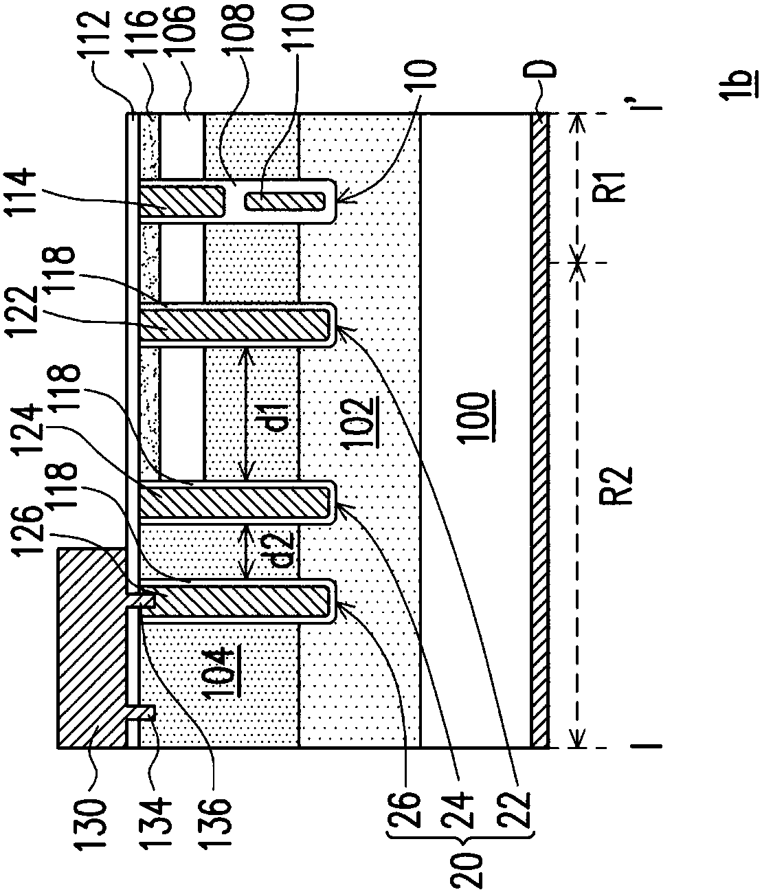
[0022] figure 1 It is a schematic top view of a power semiconductor element according to the first embodiment of the present invention. Figure 2A yes figure 1 The schematic cross-section of the line I-I'. In the following embodiments, the first conductivity type is N-type and the second conductivity type is P-type as an example for illustration, but the present invention is not limited thereto. Those skilled in the art should understand that the first conductivity type can also be P-type, and the second con...
PUM
 Abstract
Description
Claims
Application Information