A ferroelectric field effect transistor and its preparation method

An electric field effect and transistor technology, applied in the field of ferroelectric field effect transistors and their preparation, can solve problems such as reliability problems and insufficient process, and achieve the effect of promoting ferroelectricity and avoiding lattice distortion.

Active Publication Date: 2022-05-24
XIANGTAN UNIV
View PDF6 Cites 0 Cited by
  • Summary
  • Abstract
  • Description
  • Claims
  • Application Information

AI Technical Summary

Problems solved by technology

[0015] The purpose of the present invention is to provide a ferroelectric field effect transistor and its preparation method to solve the reliability problems in the preparation of ferroelectric thin films in the existing hafnium oxide-based ferroelectric field effect transistors, as well as the deficiencies in technology and other issues

Method used


Image

  • A ferroelectric field effect transistor and its preparation method
  • A ferroelectric field effect transistor and its preparation method
  • A ferroelectric field effect transistor and its preparation method

Examples


preparation example Construction

[0070] According to another aspect of the present invention, there is provided a method for preparing a ferroelectric field effect transistor, comprising:

[0071] S1: Divide the substrate layer into a source region, a drain region and an insulating region;

[0072] S2: perform ion implantation treatment in the source region and the drain region and activate the ion implantation region;

[0073] S3: sequentially arrange a gate insulating layer, a first buffer layer, an intermediate dielectric layer, a second buffer layer and a gate electrode layer on the insulating region;

[0074] S4: Etch contact holes in both the source region and the drain region, and fill the contact holes with electrodes to obtain semi-finished products with electrodes;

[0075] S5: adopting high temperature annealing to activate the intermediate dielectric layer, the first buffer layer and the second buffer layer to fully generate element diffusion and interfacial reaction on the semi-finished product ...

Embodiment 1

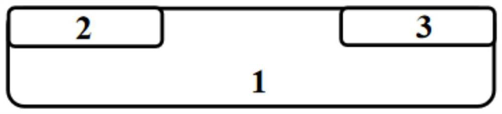
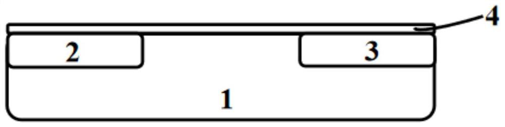
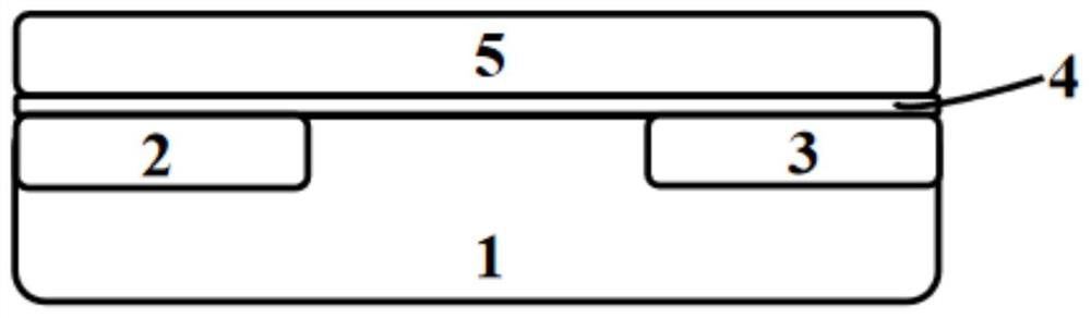
[0090] An optional embodiment of the present invention provides a ferroelectric field effect transistor that makes full use of element diffusion and interface reaction to prepare hafnium oxide-based ferroelectric field effect transistors. In this embodiment, the hafnium oxide-based ferroelectric field effect transistor includes: a horizontally arranged lining The bottom layer 1, the source region 2 and the drain region 3 located on the substrate layer 1 and separately arranged, the gate insulating layer 4 located between the source region 2 and the drain region 3, the first buffer layer 5, in the first buffer The intermediate dielectric layer 6 , the second buffer layer 7 , the gate electrode layer 8 on the layer 5 , and the source electrode 9 and the drain electrode 10 are formed on the source region 2 and the drain region 3 .

[0091] The horizontally arranged substrate layer 1 consists of p-type doped Si (p-Si) material;

[0092] The gate insulating layer 4 is made of silic...

Embodiment 2

[0108] An optional embodiment of the present invention provides a ferroelectric field effect transistor that makes full use of element diffusion and interface reaction to prepare hafnium oxide-based ferroelectric field effect transistors. In this embodiment, the hafnium oxide-based ferroelectric field effect transistor includes: a horizontally arranged lining The bottom layer 1, the source region 2 and the drain region 3 located on the substrate layer 1 and separately arranged, the gate insulating layer 4 located between the source region 2 and the drain region 3, the first buffer layer 5, in the first buffer The intermediate dielectric layer 6 , the second buffer layer 7 , the gate electrode layer 8 on the layer 5 , and the source electrode 9 and the drain electrode 10 are formed on the source region 2 and the drain region 3 .

[0109] The horizontally arranged substrate layer 1 is composed of p-type doped Si (p-Si) material;

[0110] The gate insulating layer 4 is composed o...


PUM

PropertyMeasurementUnit
thicknessaaaaaaaaaa
thicknessaaaaaaaaaa
thicknessaaaaaaaaaa

Abstract

The invention discloses a ferroelectric field effect transistor, comprising: a substrate layer, a gate insulating layer, a first buffer layer, an intermediate dielectric layer, a second buffer layer, a gate electrode layer, a source electrode and a drain electrode; the substrate layer is provided with a source electrode region, drain region, and insulating covering region, wherein the source region and the drain region are arranged at intervals; the source region is provided with a source electrode, and the drain region is provided with a drain electrode, and the insulating covering region is sequentially stacked from bottom to top. Insulation layer, first buffer layer, intermediate dielectric layer, second buffer layer and gate electrode layer. The transistor adds the first buffer layer and the second buffer layer. On the one hand, the deposition of the buffer layer can play an interface induction role, and due to the equivalent lattice matching, it can avoid causing large lattice distortion; on the other hand, in the The supporting effect of the first buffer layer and the second buffer layer is beneficial to the formation of the element-doped ferroelectric thin film and promotes the ferroelectricity of the ferroelectric thin film.

Description

technical field [0001] The invention belongs to the technical field of electronic devices, and in particular relates to a ferroelectric field effect transistor and a preparation method thereof. Background technique [0002] As a high-tech industry, the electronic information industry plays a more important role in expanding social employment, promoting economic transformation and upgrading, enhancing international competitiveness and maintaining national security. In recent years, with the continuous breakthrough and development of modern information technology, semiconductor memory represented by memory (DRAM) and flash memory (Flash) has led the development of integrated circuit technology, and has contributed to the development of information technology industry, social progress and human life style. changes have had an important impact. So far, mainstream memories such as high-density, low-cost DRAM and NAND Flash have become increasingly difficult to meet the needs of ...

Claims


Application Information

Patent Timeline
Patent Type & Authority Patents(China)
IPC IPC(8): H01L29/78H01L29/51H01L21/336H01L21/28
CPCH01L29/78391H01L29/516H01L29/6684H01L29/401
Inventor 廖敏郇延伟
Owner XIANGTAN UNIV
Why Eureka
Try Eureka