Polarizing film with added adhesive layer, polarizing film with added adhesive layer for in-cell liquid crystal panel, in-cell liquid crystal panel, and liquid crystal display device

A technology of adhesive layer and liquid crystal panel, which is applied in the field of liquid crystal display devices and embedded liquid crystal panels, which can solve the problems of unstable sensor electrode capacity, electric field disorder, and decreased sensitivity of the touch panel, and achieve good antistatic function, suppress Effect of white turbidity and suppression of poor conduction

Pending Publication Date: 2019-11-19
NITTO DENKO CORP
View PDF15 Cites 0 Cited by
  • Summary
  • Abstract
  • Description
  • Claims
  • Application Information

AI Technical Summary

Problems solved by technology

When there is a conductive layer such as an antistatic layer between the above-mentioned transparent electrode pattern and the user's finger, the electric field between the drive electrode and the sensor electrode is disturbed, the capacitance of the sensor electrode becomes unstable, the sensitivity of the touch panel decreases, and malfunction occurs. s reason

Method used


Image

  • Polarizing film with added adhesive layer, polarizing film with added adhesive layer for in-cell liquid crystal panel, in-cell liquid crystal panel, and liquid crystal display device
  • Polarizing film with added adhesive layer, polarizing film with added adhesive layer for in-cell liquid crystal panel, in-cell liquid crystal panel, and liquid crystal display device
  • Polarizing film with added adhesive layer, polarizing film with added adhesive layer for in-cell liquid crystal panel, in-cell liquid crystal panel, and liquid crystal display device

Examples


Embodiment 1~6

[0196]

[0197] A tackifier layer and an adhesive layer were sequentially formed in combinations shown in Table 1 on one side (corona-treated side) of the polarizing film obtained above to prepare a polarizing film with an adhesive layer.

[0198] In addition, in Comparative Example 6, no ionic compound was blended in the preparation of the adhesive composition.

[0199] The following evaluations were performed about the tackifier layer, the adhesive layer, and the polarizing film with an adhesive layer obtained in the said Example and the comparative example. The evaluation results are shown in Table 1 and Table 2.

[0200]

[0201] The polarizing film with an adhesive layer obtained in the Example and the comparative example was cut into 25 mm width x 50 mm length. The pressure-sensitive adhesive layer and the vapor-deposited surface of the vapor-deposited film of indium-tin oxide deposited on the surface of a 50 μm-thick polyethylene terephthalate film were bonded toge...


PUM

PropertyMeasurementUnit
thicknessaaaaaaaaaa
thicknessaaaaaaaaaa
thicknessaaaaaaaaaa

Abstract

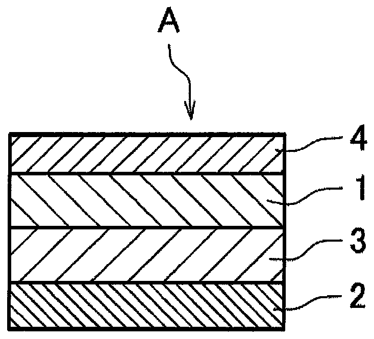
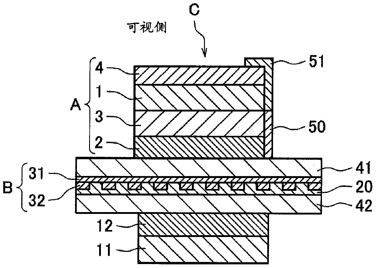
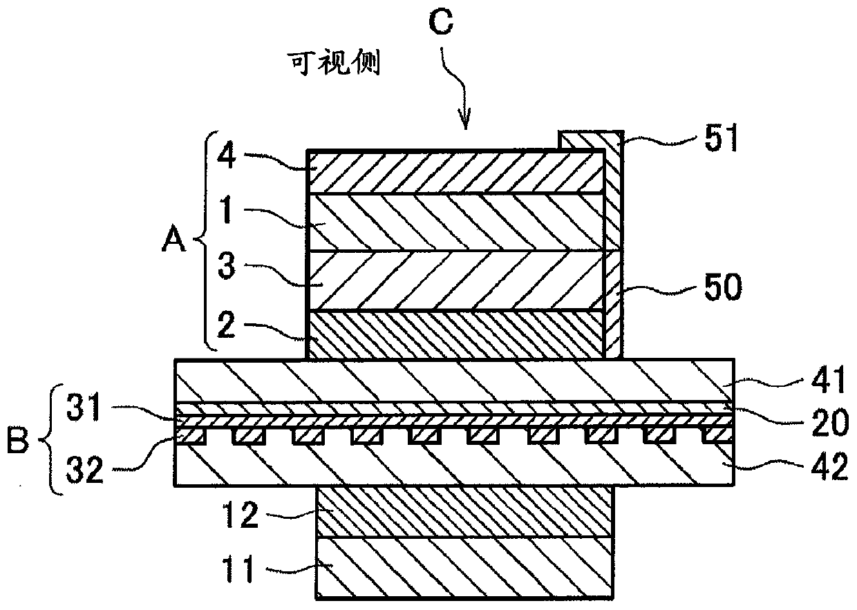
The present invention provides a polarizing film with added adhesive layer for realizing an in-cell liquid crystal panel in which the adhesion between an anchor layer and the adhesive layer is excellent, and it is possible to satisfy a stable antistatic function and touch sensor sensitivity. The polarizing film with added adhesive layer is provided with an adhesive layer and a polarizing film, andis characterized in that: the polarizing film with added adhesive layer is provided with the polarizing film, an anchor layer, and the adhesive layer in this order; the anchor layer includes a conductive polymer; the adhesive layer includes an antistatic agent; the anchor layer has a thickness of 0.01-0.5 [mu]m and a surface resistance of 1.0*108 to 1.0*1010 [omega] / square; the adhesive layer hasa thickness of 5-100 [mu]m and a surface resistance of 1.0*1010 to 1.0*1012 [omega] / square; and the ratio (b / a) of the variation in the adhesive layer-side surface resistances before and after humidification is no higher than 5.

Description

technical field [0001] The present invention relates to a polarizing film with an adhesive layer, a polarizing film with an adhesive layer for an in-cell liquid crystal panel, an in-cell liquid crystal cell in which a touch sensing function is introduced into a liquid crystal cell, and An in-cell liquid crystal panel having a polarizing film with an adhesive layer on the visible side of the in-cell liquid crystal cell. In addition, the present invention also relates to a liquid crystal display device using the above-mentioned liquid crystal panel. The liquid crystal display device with a touch sensor function using an in-cell liquid crystal panel of the present invention can be used as various input display devices such as mobile devices. Background technique [0002] A liquid crystal display device usually has a polarizing film bonded from both sides of the liquid crystal cell through an adhesive layer according to its image forming method. In addition, products in which ...

Claims


Application Information

Patent Timeline
Patent Type & Authority Applications(China)
IPC IPC(8): G02B5/30G02F1/1335G06F3/041G09F9/30G02F1/1333
CPCG02B5/30G09F9/30G06F3/0418G06F3/0412G06F2203/04103G02F1/133528G02F1/13338G02F1/136204G02F2202/22G02F2202/28C09J133/066C09J7/38C09J7/50C09J2203/318C08K5/0075C09J2301/408G02F1/1335G02B1/16G02F1/133738C09J11/06C09J133/08C09K2323/00G06F3/04182G02F1/1337
Inventor 藤田昌邦外山雄祐
Owner NITTO DENKO CORP
Why Eureka
Try Eureka