Check patentability & draft patents in minutes with Patsnap Eureka AI!

Package carrier board structure and manufacturing method thereof

A technology for encapsulating substrates and manufacturing methods, applied in semiconductor/solid-state device manufacturing, electrical components, electrical solid-state devices, etc., which can solve problems such as low yield rate, high cost, and complicated process

Active Publication Date: 2019-11-26
UNIMICRON TECH CORP
View PDF5 Cites 0 Cited by
  • Summary
  • Abstract
  • Description
  • Claims
  • Application Information

AI Technical Summary

Problems solved by technology

However, the process of the above-mentioned method is relatively complicated, the time is long, the cost is high, and it is easy to lead to disadvantages such as low yield rate of finished products.
[0003] Therefore, there is a great need for an improved package carrier structure and chip package structure, as well as its manufacturing method, which can meet the circuit design of the chip package structure with smaller, lighter and higher density, and the process of solving the above-mentioned known technologies is relatively complicated. , long time and high cost, in order to achieve high packaging efficiency, simplify the process, shorten time, reduce cost and improve the yield of finished products

Method used


Image

  • Package carrier board structure and manufacturing method thereof
  • Package carrier board structure and manufacturing method thereof
  • Package carrier board structure and manufacturing method thereof

Examples


Embodiment Construction

[0029] In order to make the description of the disclosure more detailed and complete, the following provides illustrative descriptions of the implementation aspects and specific embodiments of the present invention; but this is not the only form of implementing or using the specific embodiments of the present invention. The embodiments disclosed below can be combined or substituted for each other when beneficial, and other embodiments can also be added to one embodiment, without further description or illustration.

[0030] In the following description, numerous specific details will be set forth in order to enable readers to fully understand the following embodiments. However, embodiments of the invention may be practiced without these specific details. In other instances, well-known structures and devices are only schematically shown in order to simplify the drawings.

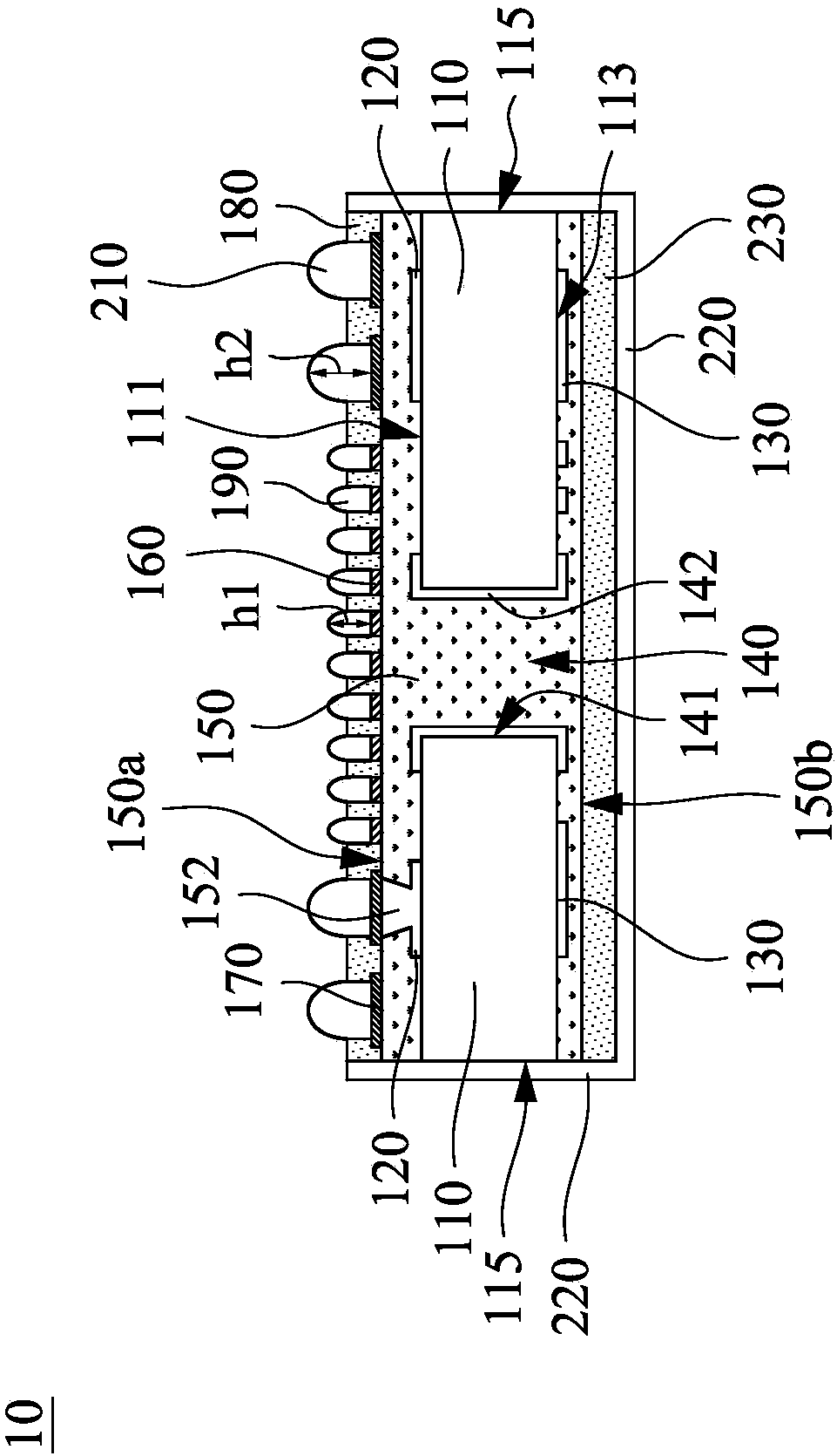
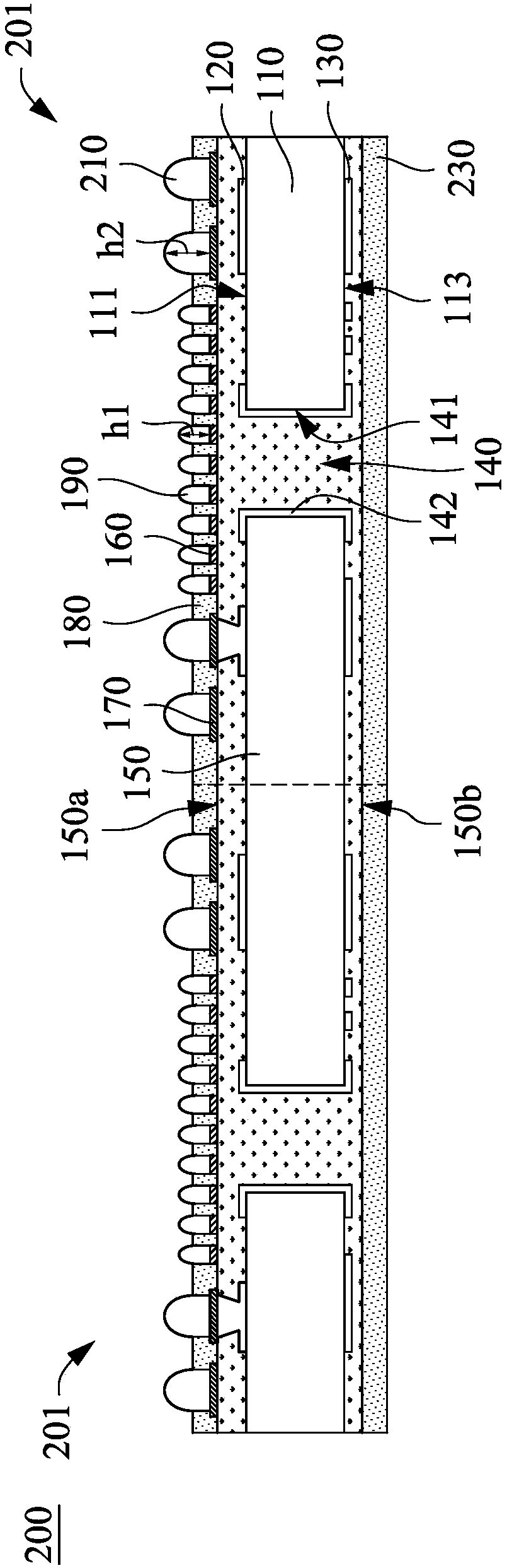
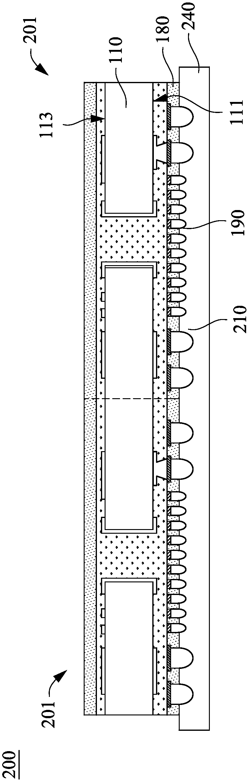
[0031] One aspect of the present invention is to provide a package carrier structure. figure 1 A schemat...


PUM


Abstract

The invention discloses a package carrier board structure and a manufacturing method thereof. The package carrier board structure includes an insulating substrate, a first circuit layer, a second circuit layer, a conductive through hole, a first conductive pad, a second conductive pad, and a first insulation layer, a first conductive structure, a second conductive structure, and a packaging layer.The first and second circuit layers are located on the upper and lower surfaces of the insulating substrate respectively. The conductive through hole penetrates through the insulating substrate and is electrically connected to the first circuit layer and the second circuit layer. The first conductive pad and the second conductive pad are electrically connected to the first circuit layer. The first insulating layer covers the insulating substrate and exposes the first and second conductive pads. The first and second conductive structures are located on the first and second conductive pads respectively. The height of the second conductive structure is greater than the height of the first conductive structure. The packaging layer covers the lower surface and the sidewall of the insulating substrate. The method of manufacturing a chip package structure can reduce the cost.

Description

technical field [0001] The invention relates to a package carrier structure and a method for manufacturing the package carrier structure. Background technique [0002] With the growing demand for lighter and more complex electronic devices, smaller, lighter and higher packaging efficiency (Packaging Efficiency) are required to meet the requirements of chip packaging. Generally, the package cutting technology commonly used in the industry is: firstly, the chip substrate is cut into multiple chip structures, and then these chip structures are placed on the substrate as the package base. At this time, the conductive structure in the chip structure is arranged relative to the substrate. Next, these chip structures are sealed with the substrate together with an encapsulation layer, and then an etching process is used to expose the conductive structures in the chip structures. Then, the encapsulation layer and the substrate located between two adjacent chip structures are cut to ...

Claims


Application Information

Patent Timeline
IPC IPC(8): H01L23/498H01L21/48
CPCH01L21/4857H01L21/486H01L23/49822H01L23/49827H01L23/49838H01L2224/11H01L2224/97
Inventor 谢育忠简俊贤陈裕华
Owner UNIMICRON TECH CORP
Features
  • R&D
  • Intellectual Property
  • Life Sciences
  • Materials
  • Tech Scout
  • Unparalleled Data Quality
  • Higher Quality Content
  • 60% Fewer Hallucinations
Learn More