Array substrate, liquid crystal display panel and display device

An array substrate and substrate substrate technology, which is applied in the field of display devices, can solve the problems of loss of aperture ratio, reduced transmittance of display panels, and greater influence of Pix' aperture ratio, so as to improve the effect of pitting.

Active Publication Date: 2019-12-03
SHANGHAI AVIC OPTOELECTRONICS
View PDF8 Cites 2 Cited by
  • Summary
  • Abstract
  • Description
  • Claims
  • Application Information

AI Technical Summary

Problems solved by technology

Although the width difference of the black matrix can be reduced by widening the width of the narrower black matrix, it has a greater impact on the...

Method used


Image

  • Array substrate, liquid crystal display panel and display device
  • Array substrate, liquid crystal display panel and display device
  • Array substrate, liquid crystal display panel and display device

Examples


Embodiment Construction

[0036] In order to make the above objects, features and advantages of the present invention more comprehensible, the present invention will be further described below in conjunction with the accompanying drawings and embodiments. Example embodiments may, however, be embodied in many forms and should not be construed as limited to the embodiments set forth herein; rather, these embodiments are provided so that this disclosure will be thorough and complete, and will fully convey the concept of example embodiments to those skilled in the art. The same reference numerals denote the same or similar structures in the drawings, and thus their repeated descriptions will be omitted. The words expressing position and direction described in the present invention are all described by taking the accompanying drawings as an example, but changes can also be made according to needs, and all changes are included in the protection scope of the present invention. The drawings of the present inv...


PUM


Abstract

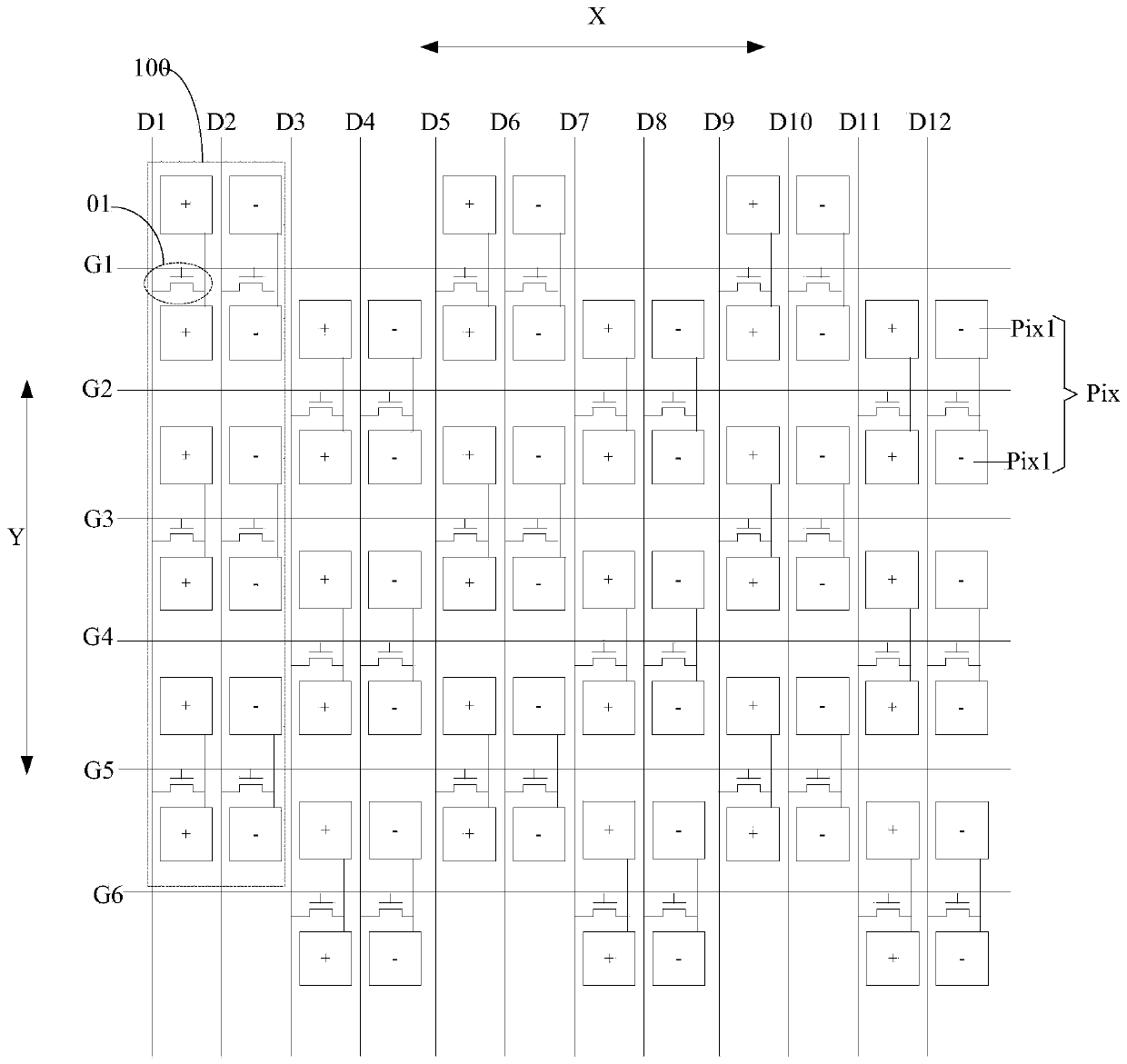
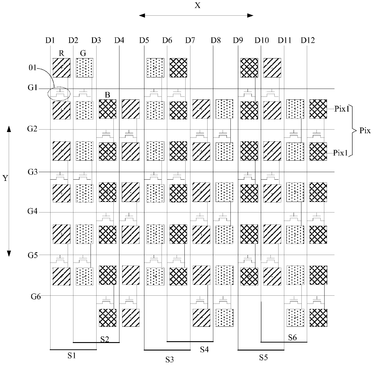
The invention discloses an array substrate, a liquid crystal display panel and a display device. Each sub-pixel comprises two sub-sub-pixels arranged in a second direction; and a switching transistorcorresponding to each sub-pixel is arranged between the two sub-sub-pixels and connected with the two sub-sub-pixels. Every two adjacent columns of sub-pixels in a first direction are used as one unitgroup; and any two adjacent unit groups are staggered by N sub-sub-pixels in the second direction. Therefore, for the overall array substrate, every two switching transistors are distributed uniformly in the second direction in each unit group. For a black matrix, one switching transistor needs to cover the widest part, so that the pocking mark feeling can be effectively improved by being compared with the prior art. Moreover, the grid lines correspondingly connected with each switching transistor are arranged between the two sub-sub-pixels in each sub-pixel; and thus in one sub-pixel, self compensating of the capacitance difference between the pixel electrode and the grid line caused by process alignment can be realized by utilizing the two sub-sub-pixels.

Description

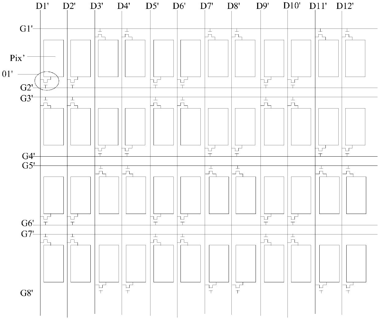
technical field [0001] The invention relates to the field of display technology, in particular to an array substrate, a liquid crystal display panel and a display device. Background technique [0002] Thin Film Transistor-Liquid Crystal Display (TFT-LCD) panels are widely used in mobile products such as mobile phones and tablet computers. Currently, in order to improve the display of vertical lines, such as figure 1 In the double-gate design shown, two gate lines Gn' are arranged between two adjacent rows of sub-pixels Pix', transistors 01' of four adjacent sub-pixels Pix' are arranged adjacent to each other, and the black matrix of the shielding transistor 01' is smaller. Wide, when displayed, there will be a sense of pitting visually. Although the width difference of the black matrix can be reduced by widening the width of the narrower black matrix, it has a greater impact on the aperture ratio of the sub-pixel Pix', which will lose more than 10% of the aperture ratio, t...

Claims


Application Information

Patent Timeline
IPC IPC(8): G02F1/1362H01L27/12
CPCG02F1/136286G02F1/13624H01L27/124G02F1/136222
Inventor 傅炯樑简守甫孙丽娜秦丹丹秦锋
Owner SHANGHAI AVIC OPTOELECTRONICS
Why Eureka
Try Eureka