Leveling and focusing device for lithography equipment

A technology for leveling, focusing, and photolithography equipment, which is applied in the field of integrated circuit equipment manufacturing, can solve the problems of easy wear of contact points and high requirements for surface treatment of contact parts, and achieve the goals of maintaining consistency, improving contact accuracy, and overcoming decoupling problems Effect

Active Publication Date: 2016-08-03
SHANGHAI MICRO ELECTRONICS EQUIP (GRP) CO LTD
View PDF5 Cites 0 Cited by
  • Summary
  • Abstract
  • Description
  • Claims
  • Application Information

AI Technical Summary

Problems solved by technology

[0005] However, the barrel-shaped design in the CN101303532 scheme of the prior art solves the problem that the roller and the cam are relatively inclined, but makes the point contact between the cam and the roller. wear and tear

Method used


Image

  • Leveling and focusing device for lithography equipment
  • Leveling and focusing device for lithography equipment
  • Leveling and focusing device for lithography equipment

Examples


Embodiment Construction

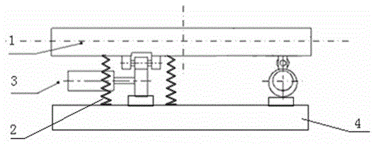
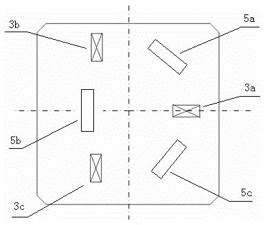
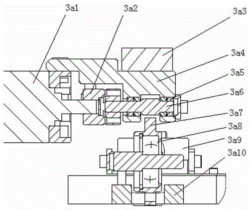
[0021] A leveling and focusing device for lithography equipment according to a specific embodiment of the present invention will be described in detail below with reference to the accompanying drawings. However, the present invention should be understood as not limited to such embodiments described below, and the technical idea of ​​the present invention can be implemented in combination with other known technologies or other technologies having the same functions as those known technologies.

[0022] In the following description, in order to clearly show the structure and working method of the present invention, many directional words will be used to describe, but "front", "rear", "left", "right", "outer", "inner" should be used Words such as ", "outward", "inward", "upper" and "lower" are to be understood as convenient terms, and should not be understood as restrictive terms. In addition, the term "X direction" used in the following description mainly refers to the direction...


PUM


Abstract

The invention discloses a leveling and focusing device for photolithography equipment, which is used to make a film carrier move vertically along Z, Rx, Ry directions. The leveling and focusing device includes a The lower cam roller device, the cam roller device includes a cam mechanism and a roller mechanism located above the cam mechanism, the roller mechanism is driven by a motor to rotate, and the cam mechanism includes a bearing mechanism for use The cam mechanism is in linear contact with the roller mechanism.

Description

technical field [0001] The invention relates to the field of integrated circuit equipment manufacturing, in particular to a leveling and focusing device for photolithography equipment. Background technique [0002] The photolithography device is the main equipment for manufacturing integrated circuits. Its function is to sequentially image different mask patterns onto the precisely aligned positions on the substrate (such as semiconductor silicon wafer or LCD panel). However, this alignment position changes due to the physical and chemical changes experienced by successive patterns, so an alignment system is needed to ensure that the alignment position of the silicon wafer corresponding to the mask can be accurately aligned every time. As the number of electronic components per unit surface area of ​​the substrate increases and the size of electronic components becomes smaller and smaller, the precision requirements for integrated circuits are increasing. Therefore, the posi...

Claims


Application Information

Patent Timeline
Patent Type & Authority Patents(China)
IPC IPC(8): G03F7/20G03F9/00
Inventor 赵娟方洁吴立伟
Owner SHANGHAI MICRO ELECTRONICS EQUIP (GRP) CO LTD
Why Eureka
Try Eureka