Display product electrode wire protection method and display product
A technology for displaying products and electrode wires, which is applied in the direction of circuits, electrical components, and electrical solid devices, and can solve problems such as bright and dark spots in the effective display area, lower product yields, and influence on the progress of mass production of products, so as to reduce display Defective problems, improve product yield, and ensure the effect of progress
- Summary
- Abstract
- Description
- Claims
- Application Information
AI Technical Summary
Problems solved by technology
Method used
Image
Examples
Embodiment 1
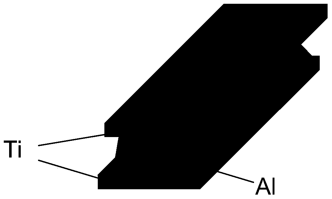
[0025] For display products, it includes at least a unit area and an IC binding area; the unit area includes an active display area (Active Area, referred to as AA area) and a marking and test area; the active display area includes anode lines and several pixel units. A part of the electrode line extends into the unit area, and the other part is in the IC binding area. Since the electrode line in the IC binding area is not covered by the thin film layer of the unit area, in the subsequent array process flow after the electrode line is prepared, The aluminum layer in the middle of the electrode line is easily etched by acid, alkali, etc. and the titanium layer above the aluminum layer is suspended, and the titanium layer of the electrode line is easy to fall off and fall into the effective display area when the electrode line is washed under high pressure, forming debris, resulting in pixel failure. The unit is damaged, causing bright and dark spots in the effective display area...
Embodiment 2
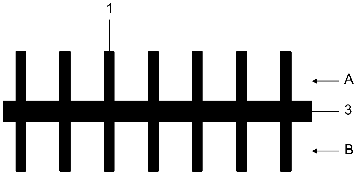
[0040] Figure 4 It is a schematic diagram of the structural design of the IC binding area of a display product provided by Embodiment 2 of the present invention. Such as Figure 4 As shown, according to another aspect of the present invention, the present invention also provides a display product, including electrode lines 1, and further comprising: a protective layer 2 formed at least in the area where the electrode lines are not covered by the unit area of the display product. In other words, there is a protective layer 2 on the part of the electrode lines 1 not covered by the display product unit area.
[0041] Further, the protective layer 2 is a silicon nitride insulating layer.
[0042] Further, the silicon nitride insulating layer has a thickness of 1000-5000A.
[0043] Further, in the IC binding area, the protective layer 2 corresponds to the shape of the electrode lines and covers all the electrode lines, and the width of the electrode lines covered by the pro...
PUM
 Abstract
Description
Claims
Application Information


