OLED array substrate, display panel and display device
A technology for array substrates and display areas, which is applied to static indicators, instruments, electrical components, etc., can solve problems affecting the overall consistency of the screen, and achieve the effects of strong process feasibility, small area, and space saving
- Summary
- Abstract
- Description
- Claims
- Application Information
AI Technical Summary
Problems solved by technology
Method used
Image
Examples
Embodiment Construction
[0076] Reference will now be made in detail to the exemplary embodiments, examples of which are illustrated in the accompanying drawings. When the following description refers to the accompanying drawings, the same numerals in different drawings refer to the same or similar elements unless otherwise indicated. The implementations described in the following exemplary examples do not represent all implementations consistent with the present invention. Rather, they are merely examples of apparatuses and methods consistent with aspects of the invention as recited in the appended claims.
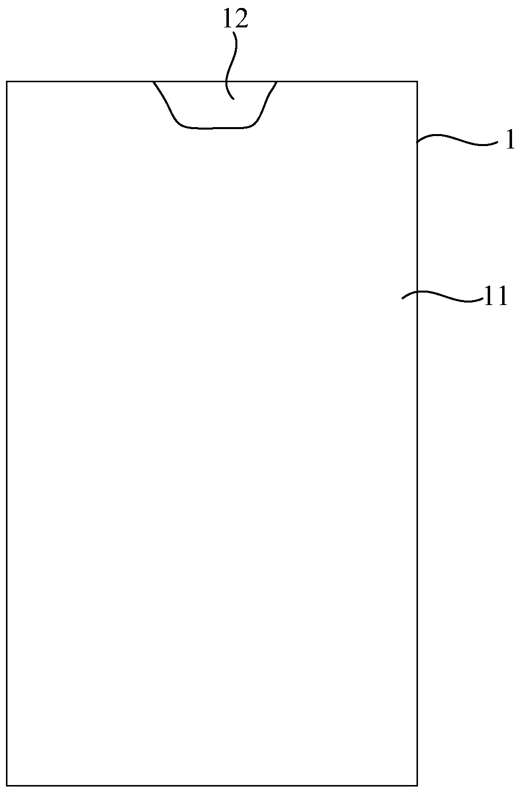
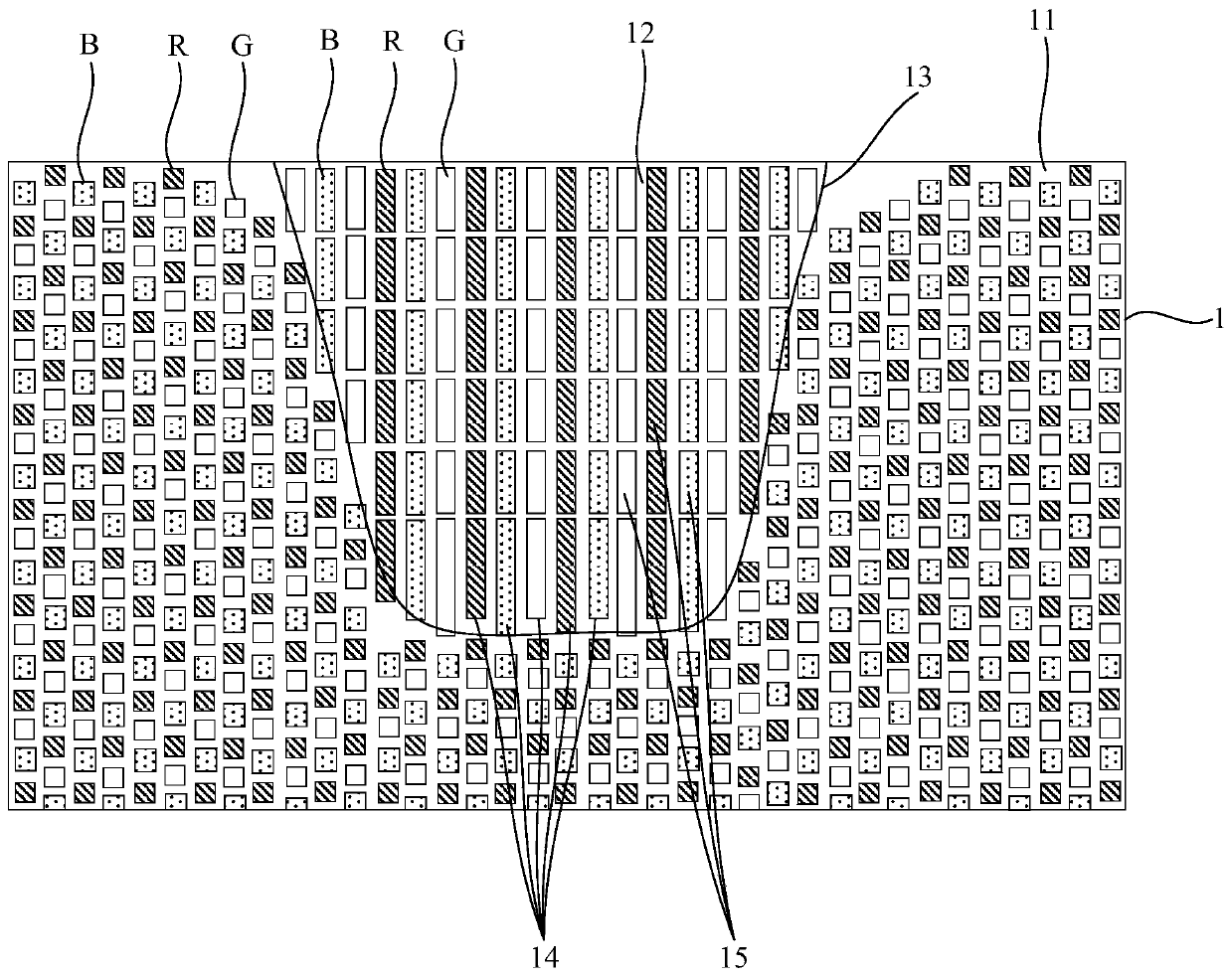
[0077] related technologies, such as figure 1 As shown, there is a full screen 1 including a non-transparent display area 11 and a transparent display area 12 , and the transparent display area 12 can realize both a light transmission function and a display function. Wherein, photosensitive elements such as a camera and a distance sensor are arranged below the transparent display area 12 . The...
PUM
 Abstract
Description
Claims
Application Information


