Supercharge Your Innovation With Domain-Expert AI Agents!

Optical device, optical ic chip, wafer, optical transceiver module and method for manufacturing optical device

A chip and optical receiver technology, applied in electromagnetic transceivers, testing of machine/structural components, optical components, etc., can solve the problems of reducing the reliability of measurement results, large losses, and large changes

Active Publication Date: 2021-02-19
FUJITSU OPTICAL COMPONENTS LTD
View PDF2 Cites 0 Cited by
  • Summary
  • Abstract
  • Description
  • Claims
  • Application Information

AI Technical Summary

Problems solved by technology

However, the loss of TM wave in the grating coupler is large
Thus, in figure 2 In the configuration shown, variations caused by wafers or optical IC chips become large and reduce the reliability of measurement results

Method used


Image

  • Optical device, optical ic chip, wafer, optical transceiver module and method for manufacturing optical device
  • Optical device, optical ic chip, wafer, optical transceiver module and method for manufacturing optical device
  • Optical device, optical ic chip, wafer, optical transceiver module and method for manufacturing optical device

Examples


no. 1 approach

[0029] Figure 4 An example of the optical IC chip according to the first embodiment is shown. In this example, the optical IC chip 1 is equipped with a device region in which an optical device is formed and a GC region in which a grating coupler or the like is formed, such as Figure 4 shown. Here, a dicing line is prepared between the device region and the GC region. That is, after the testing of the optical device is completed, the GC region is cut off from the device region.

[0030] In the example described below, the optical device is equipped with the optical receiver 10 and the optical modulator 20, but the present invention is not limited to this configuration. That is, the optical device may be configured to be equipped with the optical receiver 10 or the optical modulator 20 . Meanwhile, the optical receiver 10 and the optical modulator 20 are each an example of an optical device circuit formed on an optical IC chip.

[0031] In the device region, the optical r...

no. 2 approach

[0052] exist Figure 4 In the configuration shown in , in addition to the device region for forming the optical device, the GC region is required to form the grating coupler and the like. Therefore, the number of optical IC chips that can be formed on one wafer is reduced. The second embodiment addresses or alleviates this problem.

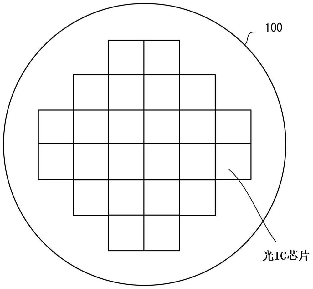
[0053] Image 6 An example of an optical IC chip according to the second embodiment is shown. Image 6 Three photo IC chips 1 a to 1 c arranged in series among the plurality of photo IC chips formed on the wafer are shown.

[0054] The configuration of each of the optical IC chips 1 ( 1 a to 1 c ) is substantially the same as each other. That is, each optical IC chip 1 is equipped with an optical receiver 10, an optical modulator 20, optical waveguides 11, 21, 22, grating couplers 61 to 65, polarization rotators 66, 69, polarization beam combiner 67, and Polarizing beam splitter 68 . exist Image 6 , the dotted line connected to the optical...

no. 3 approach

[0067] Figure 9 An example of an optical IC chip according to the third embodiment is shown. Figure 9 The illustrated optical IC chip 1 has a device region and a GC region in a similar manner to the first embodiment, but the third embodiment is not limited to this configuration. That is, the optical IC chip according to the third embodiment can be constructed without a GC region but to form a grating coupler circuit in the same manner as the second embodiment.

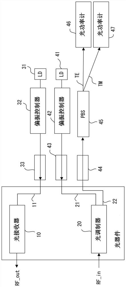
[0068] In addition to the optical receiver 10 and the optical modulator 20, a branch coupler 101 is formed in the device region. The branch coupler 101 is optically coupled to the optical receiver 10 and the optical modulator 20 . Then, when the TE wave CW light output from the polarization controller 42 is given to the optical IC chip 1 via the optical fiber array 102 , the branch coupler 101 divides and guides the TE wave CW light to the optical receiver 10 and the optical modulator 20 . Meanwhile, the optical r...


PUM


Abstract

An optical device, an optical IC chip, a wafer, an optical transceiver module and a method for manufacturing the optical device. Optical devices are formed on optical IC chips. The optical device comprises: an optical device circuit; a first optical waveguide coupled to the optical device circuit, a first grating coupler, a second grating coupler, a polarization rotator coupled to the first grating coupler, a polarization rotator coupled to the polarization rotator and a polarization beam combiner or polarization beam splitter of the second grating coupler, and a second optical waveguide coupled to the polarization beam combiner or polarization beam splitter. The first optical waveguide and the second optical waveguide respectively extend to the edge of the optical IC chip.

Description

technical field [0001] Embodiments discussed herein relate to optical devices, optical transceiver modules, and methods of manufacturing optical devices. Background technique [0002] figure 1 An example of a test method for an optical device is shown. In this example, the optical device 1 is equipped with an optical receiver 10 and an optical modulator 20 . The optical receiver 10 and the optical modulator 20 are implemented on an optical IC chip. At the same time, the optical waveguide 11 guides the input optical signal to the optical receiver 10 . The optical waveguide 21 guides the input CW (continuous wave) light to the optical modulator 20 . The optical waveguide 22 propagates the modulated optical signal generated by the optical modulator 20 . [0003] In the test of the optical receiver 10, the light source (LD) 31 outputs an optical signal. The polarization controller 32 controls the polarization of the optical signal output from the light source 31 . For exa...

Claims


Application Information

Patent Timeline
Patent Type & Authority Patents(China)
IPC IPC(8): G02B6/124G02B6/126G02B6/13G02B6/42
CPCG02B6/124G02B6/126G02B6/13G02B6/4204G02B6/4213H04B10/0731H04B10/40H04J14/06G01M11/33G01J1/0228G01J1/0429G01M11/00G02B6/12004G02B2006/12107G01J4/04H04B10/2589
Inventor 杉山昌树
Owner FUJITSU OPTICAL COMPONENTS LTD
Features
  • R&D
  • Intellectual Property
  • Life Sciences
  • Materials
  • Tech Scout
  • Unparalleled Data Quality
  • Higher Quality Content
  • 60% Fewer Hallucinations
Learn More