Three-dimensional memory structure and preparation method thereof

A memory, three-dimensional technology, applied in the direction of semiconductor devices, electrical solid devices, electrical components, etc., can solve the problem of increasing gate word line resistance, achieve the effects of reducing resistance, improving device performance, and relieving stress

Active Publication Date: 2020-02-18
YANGTZE MEMORY TECH CO LTD
View PDF9 Cites 3 Cited by
  • Summary
  • Abstract
  • Description
  • Claims
  • Application Information

AI Technical Summary

Problems solved by technology

[0005] In view of the above-mentioned shortcomings of the prior art, the purpose of the present invention is to provide a three-dimensional memory structure and its preparation method to solve the problems in the prior art such as the increase of gate word line resistance caused by compressing the height of the sacrificial layer

Method used


Image

  • Three-dimensional memory structure and preparation method thereof
  • Three-dimensional memory structure and preparation method thereof
  • Three-dimensional memory structure and preparation method thereof

Examples


Embodiment 1

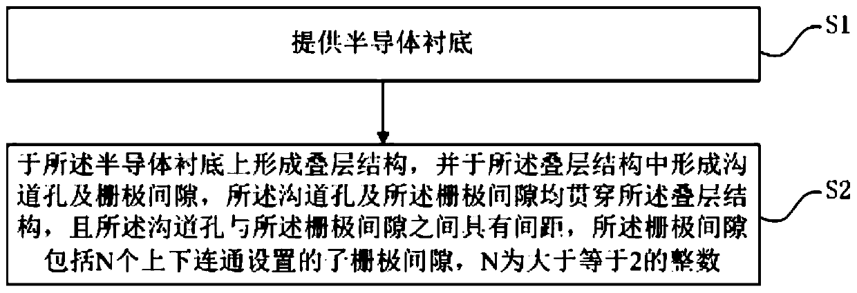
[0107] Such as figure 1 As shown, the present invention provides a method for preparing a three-dimensional memory structure, comprising the following steps:

[0108] Provide semiconductor substrates;

[0109] forming a stacked structure on the semiconductor substrate, and forming a channel hole and a gate spacer in the stacked structure, the channel hole and the gate spacer both passing through the stacked structure, In addition, there is a distance between the channel hole and the gate spacer, and the gate spacer includes N sub-gate spacers connected up and down, where N is an integer greater than or equal to 2.

[0110] The preparation process of the three-dimensional memory structure in the present invention will be described in detail below in conjunction with the accompanying drawings.

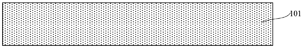
[0111] Such as figure 1 S1 and figure 2 As shown, a semiconductor substrate is provided.

[0112] Specifically, the semiconductor substrate 101 can be selected according to the act...

Embodiment 2

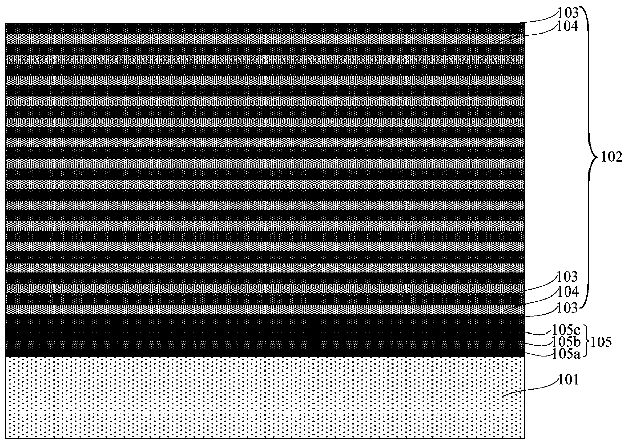
[0168] Such as Figure 22 and Figure 23 shown, refer to Figure 1-21 , the present invention also provides a three-dimensional memory structure, the three-dimensional memory structure is preferably prepared by the preparation method of the present invention, the three-dimensional memory structure includes:

[0169] semiconductor substrate 101; and

[0170] The stack structure 118 is formed on the semiconductor substrate 101, the channel hole 106 and the gate spacer 107 are formed in the stack structure 118, and the stack structure 118 includes alternately stacked gate layers and insulating dielectric layers 103, the channel hole 106 and the gate spacer 107 both pass through the stacked structure 118, and there is a distance between the channel hole 106 and the gate spacer 107, and the gate spacer 107 includes N sub-gate isolation grooves 107a connected up and down, where N is an integer greater than or equal to 2.

[0171] Specifically, the semiconductor substrate 101 can...


PUM


Abstract

The invention provides a three-dimensional memory structure and a preparation method thereof. The preparation method comprises the following steps: providing a semiconductor substrate; forming a laminated structure on the semiconductor substrate and forming a channel hole and a gate spacing groove in the laminated structure, wherein the gate spacing groove includes N sub-gate spacing grooves whichare vertically communicated, and N is an integer greater than or equal to 2. The gate spacing grooves of the three-dimensional memory are prepared into a structure including at least two sub-gate spacing grooves which are vertically communicated, the arrangement of a plurality of the sub-gate spacing grooves makes the preparation of the single sub-gate spacing groove easy to control, the key sizecan be reduced, the distance between the channel hole and the gate spacing groove can be further increased, the length of the subsequent gate layer can be increased, the resistance of the gate layercan be reduced, the device speed can be improved and the device performance can be optimized. The gate spacing groove cavity is prepared in the gate spacing groove so that the stress brought by the material layer can be relieved, the stress of the whole device structure can be relieved, the device resistance can be reduced and the device performance can be improved.

Description

technical field [0001] The invention belongs to the field of semiconductor design and manufacture, and in particular relates to a three-dimensional memory structure and a preparation method thereof. Background technique [0002] With the development of planar flash memory, the production process of semiconductors has made great progress. However, in recent years, the development of planar flash memory has encountered various challenges: physical limits, existing development technology limits, and storage electron density limits. In this context, in order to solve the difficulties encountered by planar flash memory and pursue lower unit storage In order to reduce the production cost of the unit, a three-dimensional memory structure emerges as the times require. The three-dimensional memory structure can enable each memory die in the memory device to have a greater number of memory units. [0003] In non-volatile memory, such as NAND memory, one way to increase the memory den...

Claims


Application Information

Patent Timeline
Patent Type & Authority Applications(China)
IPC IPC(8): H01L27/11524H01L27/11556H01L27/1157H01L27/11582
CPCH10B41/35H10B41/27H10B43/35H10B43/27
Inventor 左明光万先进朱宏斌
Owner YANGTZE MEMORY TECH CO LTD
Why Eureka
Try Eureka