Supercharge Your Innovation With Domain-Expert AI Agents!

Memory device and memory peripheral circuit

A peripheral circuit and memory technology, applied in static memory, instruments, etc., can solve the problems of large configuration space for metal fuses, failure to return to state, difficulty in applying miniaturized memory devices, etc., and achieve the effect of reducing layout space

Active Publication Date: 2020-03-06
WINBOND ELECTRONICS CORP
View PDF4 Cites 1 Cited by
  • Summary
  • Abstract
  • Description
  • Claims
  • Application Information

AI Technical Summary

Problems solved by technology

However, once the metal fuse is blown or turned on, it cannot go back to the state before the redundant row operation
In addition, metal fuses require a large configuration space, making it difficult to apply to miniaturized memory devices

Method used


Image

  • Memory device and memory peripheral circuit
  • Memory device and memory peripheral circuit
  • Memory device and memory peripheral circuit

Examples


Embodiment Construction

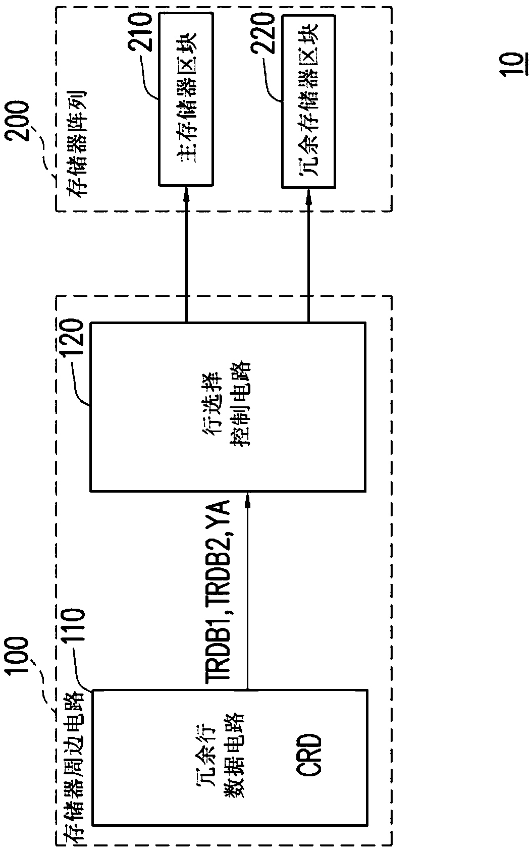
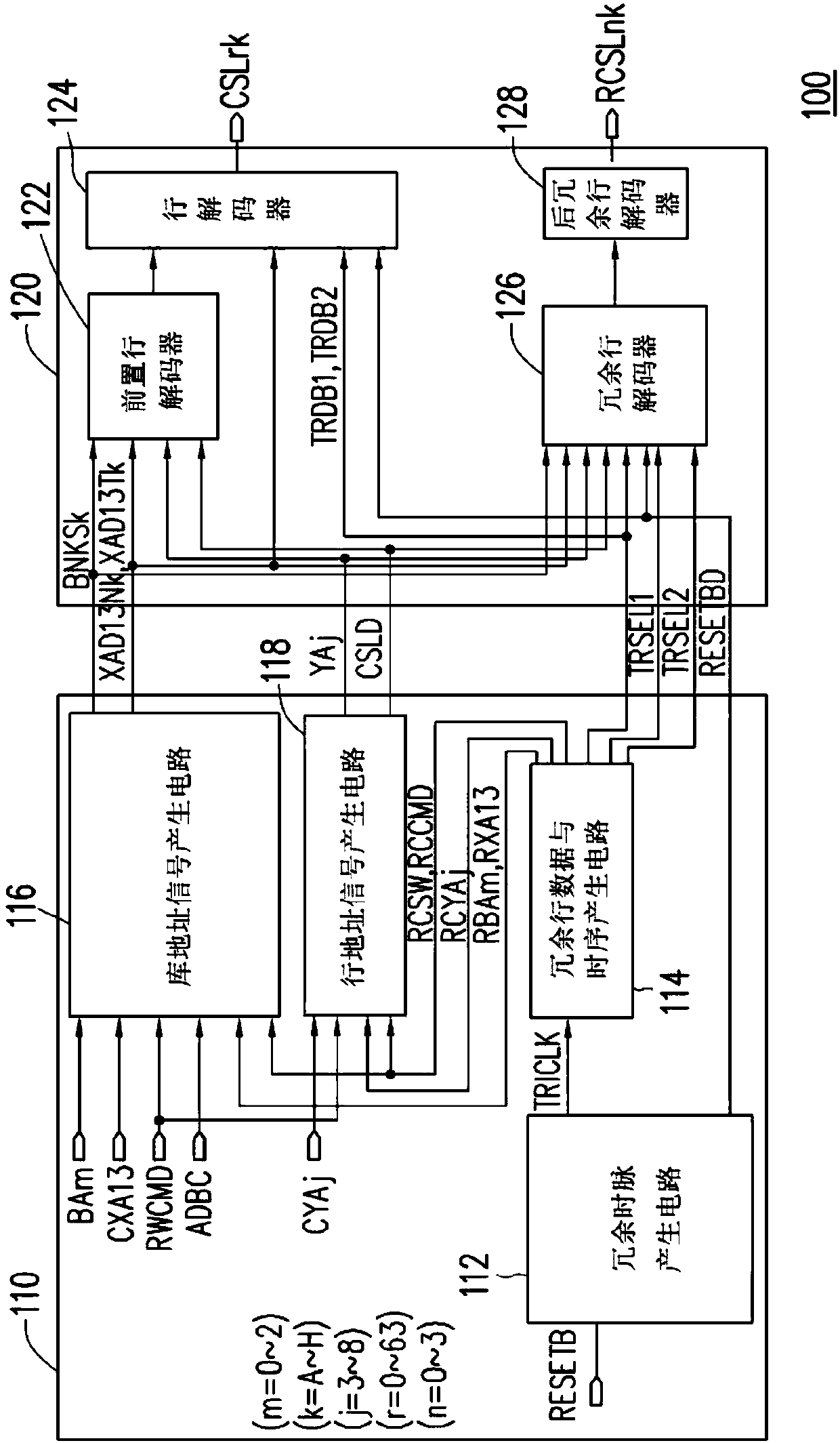
[0067] Please refer to figure 1, the memory device 10 includes a memory peripheral circuit 100 and a memory array 200 . The memory peripheral circuit 100 includes a redundant row data circuit 110 and a row selection control circuit 120 . The memory array 200 includes a main memory block 210 and a redundant memory block 220 . The redundant row data circuit 110 is used for storing redundant row information CRD. The redundancy row information CRD records the addresses of bad rows detected in the main memory block 210 during the test phase. The redundant row data circuit 110 provides the redundant test data signals TRDB1 and TRDB2 and the row address signal YA to the row selection control circuit 120 according to the redundant row information CRD. The row address signal YA includes a redundant row address signal, which is the row address signal YA corresponding to the redundant test data signals TRDB1, TRDB2. The row selection control circuit 120 is coupled between the redunda...


PUM


Abstract

The invention provides a memory device and a memory peripheral circuit. The memory peripheral circuit includes a redundant row data circuit and a row selection control circuit. The redundant row datacircuit is configured to provide a redundant test data signal and a row address signal. The row address signal includes a redundant row address signal. The row selection control circuit comprises a row decoder and a redundant row decoder. The row decoder disables the bad row address of the main memory block according to the redundant test data signal and the redundant row address signal. The redundant row decoder is used for latching the redundant row address signal, comparing the row address signal with the latched redundant row address signal to obtain a comparison result, and enabling the redundant row address of the redundant memory block according to the comparison result.

Description

technical field [0001] The present invention relates to a memory device and a memory peripheral circuit, in particular to a memory device and a memory peripheral circuit for replacing bad row addresses with redundant row addresses. Background technique [0002] In the redundant row operation of a general memory device, metal fuses can be configured in each row decoder, and bad row addresses can be disabled by turning on or blowing the metal fuses. However, once the metal fuse is blown or turned on, it cannot return to the state before the redundant row operation. In addition, metal fuses require a relatively large configuration space, making it difficult to apply them in miniaturized memory devices. Contents of the invention [0003] The present invention provides a memory device and a memory peripheral circuit. The memory peripheral circuit of the memory device is configured to disable the bad row address of the memory device, thereby replacing the existing metal fuse. ...

Claims


Application Information

Patent Timeline
Patent Type & Authority Applications(China)
IPC IPC(8): G11C29/00
CPCG11C29/835G11C29/838
Inventor 中冈裕司
Owner WINBOND ELECTRONICS CORP
Features
  • R&D
  • Intellectual Property
  • Life Sciences
  • Materials
  • Tech Scout
  • Unparalleled Data Quality
  • Higher Quality Content
  • 60% Fewer Hallucinations
Learn More