Check patentability & draft patents in minutes with Patsnap Eureka AI!

CMOS voltage reference circuit with ultralow linear sensitivity

A voltage reference and sensitivity technology, which is applied in the direction of adjusting electric variables, control/regulation systems, instruments, etc., can solve the problems of difficult operation of bandgap reference circuits, achieve low linear sensitivity voltage references, low voltage references, and save circuit costs Effect

Active Publication Date: 2020-03-13
SOUTHEAST UNIV
View PDF3 Cites 4 Cited by
  • Summary
  • Abstract
  • Description
  • Claims
  • Application Information

AI Technical Summary

Problems solved by technology

Due to the need to use BJT devices in the bandgap reference voltage, affected by the characteristics of the BJT device itself, it is difficult for the bandgap reference circuit to work under low voltage conditions

Method used


Image

  • CMOS voltage reference circuit with ultralow linear sensitivity
  • CMOS voltage reference circuit with ultralow linear sensitivity
  • CMOS voltage reference circuit with ultralow linear sensitivity

Examples


Embodiment Construction

[0016] Embodiments of the present invention will be described below in conjunction with the accompanying drawings.

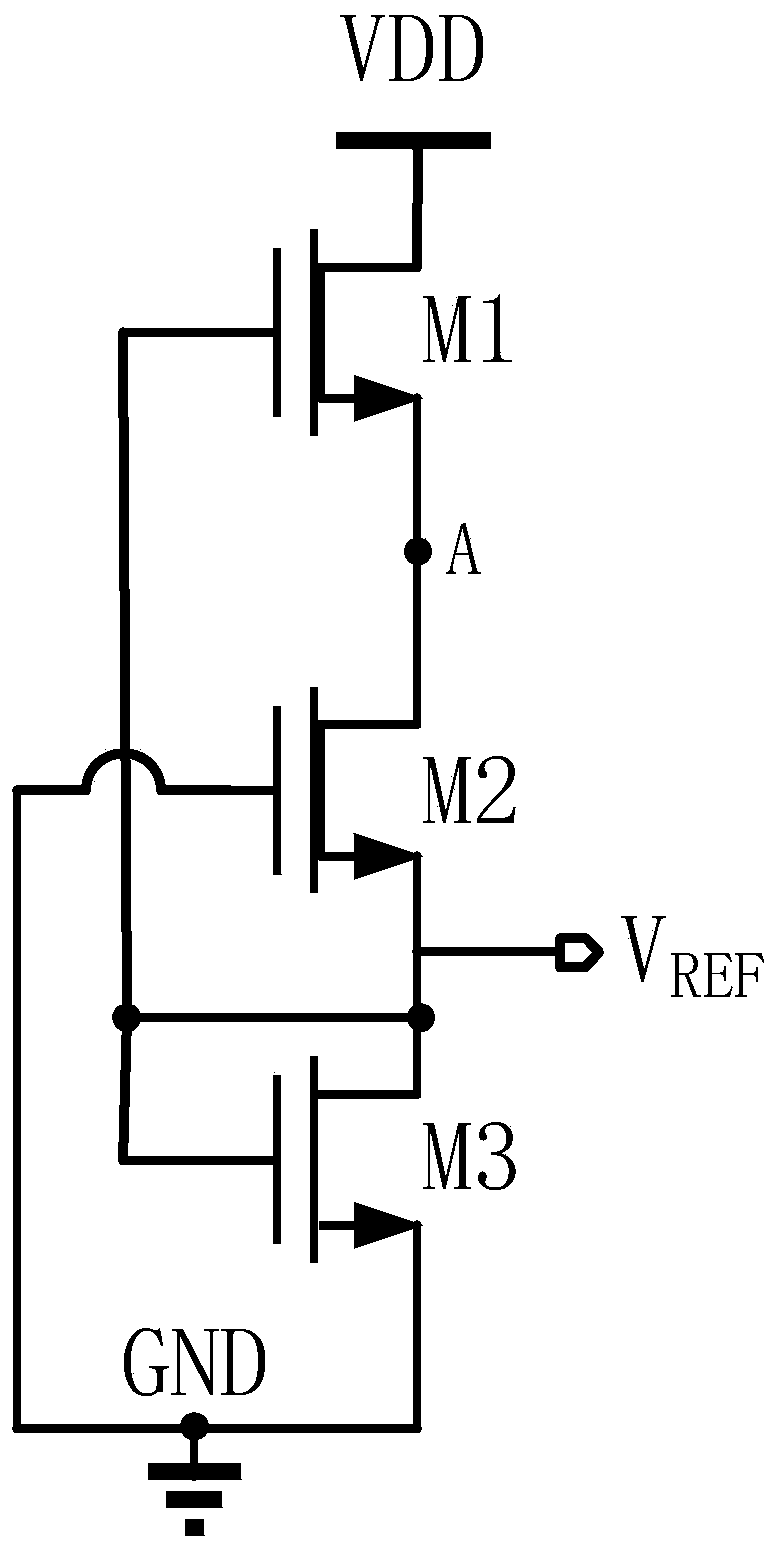
[0017] Such as figure 1 As shown, the present invention designs a CMOS voltage reference circuit with ultra-low linear sensitivity, including: a first intrinsic NMOS transistor M1, a second intrinsic NMOS transistor M2, a standard NMOS transistor M3, and the circuit also includes an input signal VDD and an output Reference voltage V REF .

[0018] Wherein, the input signal VDD of the CMOS voltage reference circuit is connected to the drain of the first intrinsic NMOS transistor M1, the gate of the first intrinsic NMOS transistor M1 is respectively connected to the gate and drain of the standard NMOS transistor M3, and the standard NMOS The drain of tube M3 is connected to the output reference voltage V REF connected, and the source of the first intrinsic NMOS transistor M1 is connected to the drain of the second intrinsic NMOS transistor M2; the gate of the s...


PUM


Abstract

The invention discloses a CMOS voltage reference circuit with ultralow linear sensitivity. The circuit comprises a first intrinsic NMOS tube M1, a second intrinsic NMOS tube M2 and a standard NMOS tube M3; an input signal VDD is connected with a drain electrode of the first intrinsic NMOS tube M1; the grid electrode of the first intrinsic NMOS tube M1 is connected with the grid electrode and the drain electrode of the standard NMOS tube M3; the drain electrode of the standard NMOS tube M3 is connected with output reference voltage VREF,; the source electrode of the first intrinsic NMOS tube M1is connected with the drain electrode of the second intrinsic NMOS tube M2; the grid electrode of the second intrinsic NMOS tube M2 is connected with a ground signal GND; the source electrode of thesecond intrinsic NMOS tube M2 is connected with the drain electrode of the standard NMOS tube M3 and an output reference voltage VREF; and the source electrode of the standard NMOS tube M3 is connected with a ground signal GND. According to the invention, the linear sensitivity of the voltage reference can be effectively reduced, so that the influence of the power supply voltage on the voltage reference is suppressed, and meanwhile, the chip area can be reduced, thereby saving the circuit cost.

Description

technical field [0001] The invention relates to a CMOS voltage reference circuit with ultra-low linear sensitivity, belonging to the technical field of voltage references. Background technique [0002] The voltage reference module is an important basic module in both analog circuits and digital-analog hybrid circuits. The voltage reference needs to provide a reference voltage that does not change with the process, power supply voltage and temperature. With the development of high integration and low power consumption, the design of voltage reference is more stringent. At low voltage, the design of the voltage reference will have more difficulties. [0003] Now the main voltage reference can be divided into bandgap reference voltage and CMOS reference voltage. Since BJT devices are needed in the bandgap reference voltage, affected by the characteristics of the BJT device itself, it is difficult for the bandgap reference circuit to work at a low voltage. Therefore, a voltag...

Claims


Application Information

Patent Timeline
IPC IPC(8): G05F1/56
CPCG05F1/56
Inventor 吴建辉吴志强谢祖帅周全才瞿剑李红
Owner SOUTHEAST UNIV
Features
  • R&D
  • Intellectual Property
  • Life Sciences
  • Materials
  • Tech Scout
  • Unparalleled Data Quality
  • Higher Quality Content
  • 60% Fewer Hallucinations
Learn More