Buffer area management method for NAND flash memory
A management method and buffer technology, applied in the cache field of computer storage devices, can solve problems such as asymmetric read and write costs of NAND flash memory, and achieve the effects of avoiding performance jitter problems, reducing search overhead and high hit rate.
- Summary
- Abstract
- Description
- Claims
- Application Information
AI Technical Summary
Problems solved by technology
Method used
Image
Examples
Embodiment Construction
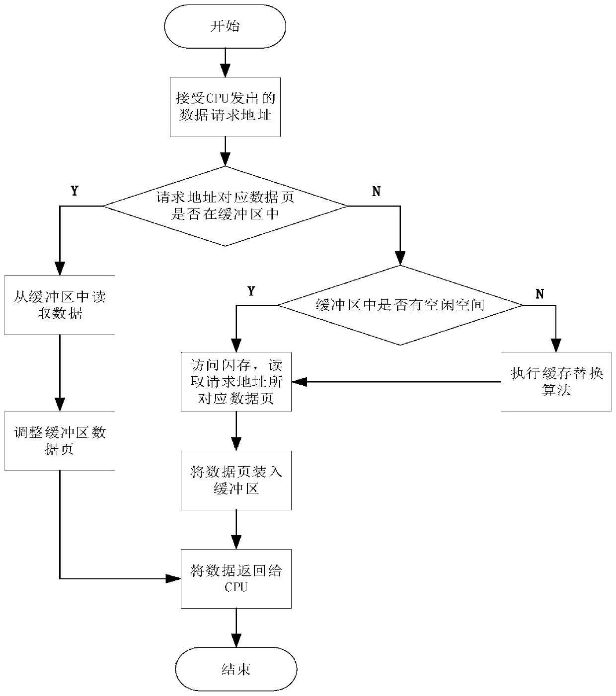
[0042] see figure 1 , a buffer management method for NAND flash memory, the specific steps are as follows:
[0043] S1, the system counter is set, and the system counter value is used as the access time stamp value of the accessed data page in the buffer;
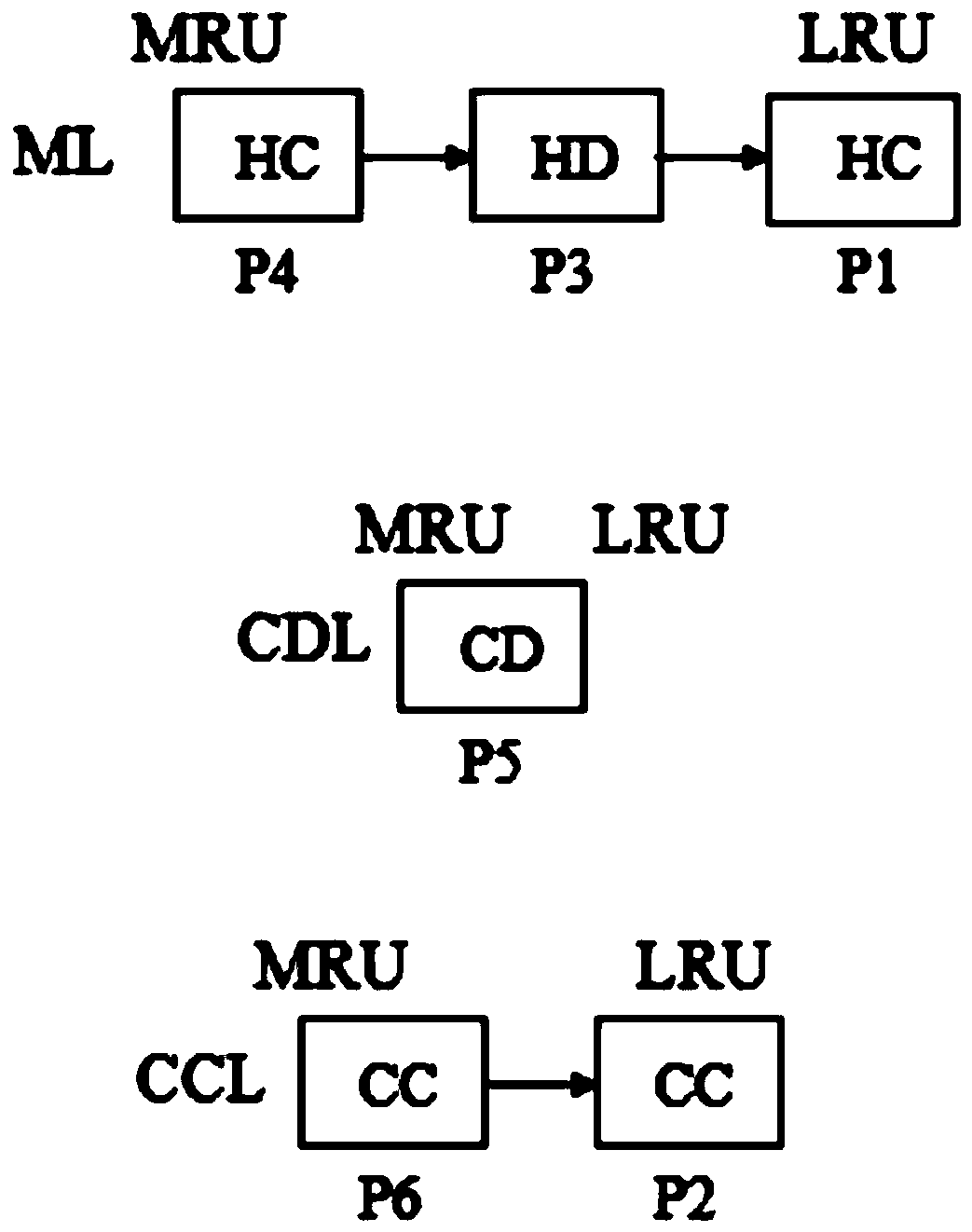
[0044] In terms of overall logic, the organizational structure of the buffer is regarded as an LRU linked list organized according to the logical number of the data page. The data page at the MRU end of the logical LRU linked list is the data page currently being accessed by the system, and its access time stamp value is the largest. The value is equal to the current system counter value, and from the MRU end to the LRU end, the data page access time stamp value decreases in turn.
[0045] On this basis, the concept of time window is proposed, and a time window size is selected at the MRU end of the logical LRU linked list to identify the number of data pages that have been accessed in the most recent period. The time wind...
PUM
 Abstract
Description
Claims
Application Information


