Display plasma module with double-layer exposure structure and manufacturing method thereof

A plasma and double-layer technology, applied in optics, nonlinear optics, instruments, etc., can solve problems such as spacer particle instability, affecting display effects, displaying disordered flow of plasma, etc.

Pending Publication Date: 2020-03-24
WUXI VISION PEAK TECH
View PDF0 Cites 1 Cited by
  • Summary
  • Abstract
  • Description
  • Claims
  • Application Information

AI Technical Summary

Problems solved by technology

The disadvantage of this structure is that because the spacer particles are unstable, they will break away from the cofferdam when pressed or squeezed, so they cannot support the display plasma module and control the thickness of the display plasma module, resulting in the disordered flow of display plasma and affecting the display. Effect

Method used


Image

  • Display plasma module with double-layer exposure structure and manufacturing method thereof
  • Display plasma module with double-layer exposure structure and manufacturing method thereof
  • Display plasma module with double-layer exposure structure and manufacturing method thereof

Examples


Embodiment Construction

[0038] In order to make the object, technical solution and advantages of the present invention clearer, the present invention will be described in further detail below in conjunction with specific embodiments and with reference to the accompanying drawings. Wherein the same components are denoted by the same reference numerals. It should be noted that the words "front", "rear", "left", "right", "upper" and "lower" used in the following description refer to directions in the drawings. The terms "inner" and "outer" are used to refer to directions toward or away from, respectively, the geometric center of a particular component.

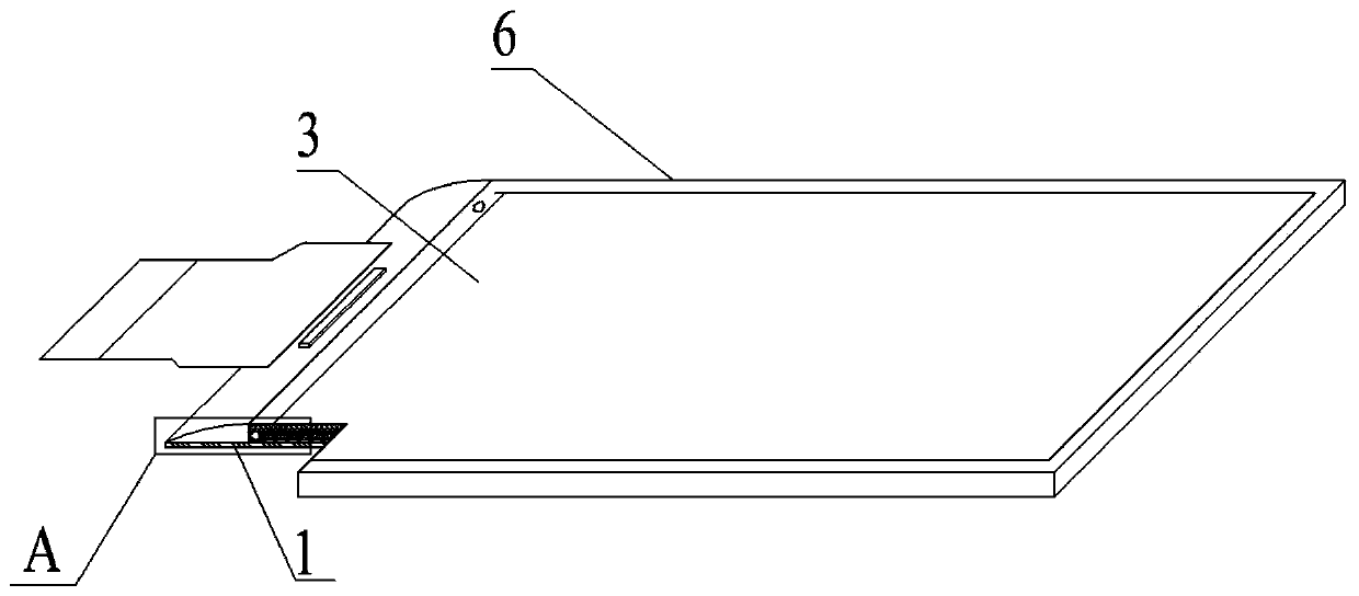
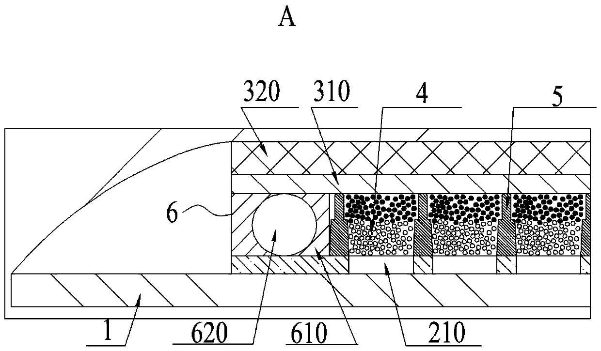
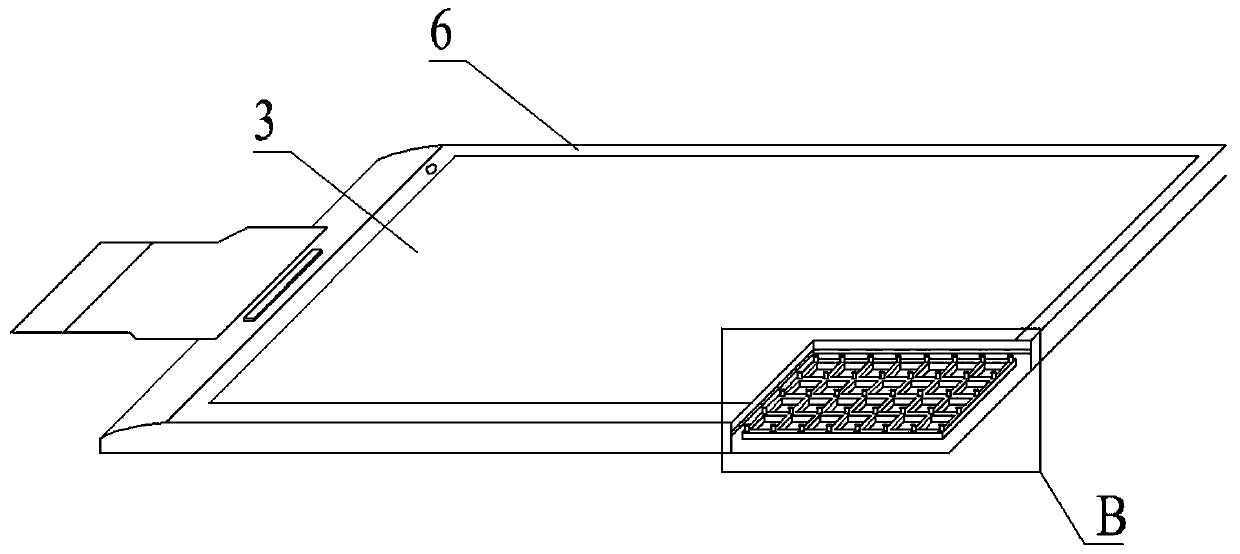
[0039] As a first aspect of the present invention, a display plasma module with a double-layer exposure structure is provided, such as figure 1 and figure 2 As shown, the display plasma module of the double-layer exposure structure includes:

[0040] A substrate 1, the substrate 1 includes a display area and a pad frame area surrounding the outer pe...


PUM

PropertyMeasurementUnit
diameteraaaaaaaaaa
heightaaaaaaaaaa
heightaaaaaaaaaa

Abstract

The invention relates to the field of electronic display, in particular to a display plasma module with a double-layer exposure structure and a manufacturing method of the display plasma module. The display plasma module of the double-layer exposure structure comprises a substrate which comprises a display area and a gasket frame area surrounding the periphery of the display area; a lower electrode which is arranged in the display area, and comprises a plurality of pixel lower electrodes which are arranged in an array mode; an upper electrode which is arranged on the lower electrode; a displayplasma which is filled between the upper electrode and the lower electrode; a plasma blocking and separating frame which is arranged in the display plasma and comprises a plurality of unit frames, wherein each unit frame is correspondingly arranged at the periphery of the pixel lower electrode, and a supporting column is arranged on each unit frame; and a gasket frame which is arranged in the gasket frame area, wherein the lower end of the gasket frame is coupled and sealed with the substrate, and the upper end is coupled and sealed with the upper electrode. According to the present invention, the display effect can be improved.

Description

technical field [0001] The invention relates to the field of electronic display, in particular to a display plasma module with a double-layer exposure structure and a manufacturing method thereof. Background technique [0002] In the existing display plasma module with double-layer microstructure, a patterned structure of cofferdam is manufactured on the surface of thin film transistor (Thin Film Transistor, TFT). The cofferdam covers the gap between adjacent pixel electrodes, and the cofferdam structure After the formation, the spacer particles are further sprayed to form a layer of spacer particles on the cofferdam. Since the weight of the spacer particles is about 1 / 5 of the display plasma ball, they can float on the display plasma. When the transparent base layer is pressed on the liner frame, most of the spacer particles are squeezed, transferred and adsorbed above the cofferdam to form a spacer particle layer. The disadvantage of this structure is that because the spa...

Claims


Application Information

Patent Timeline
Patent Type & Authority Applications(China)
IPC IPC(8): G02F1/167G02F1/16753G02F1/1679
CPCG02F1/167G02F1/16753G02F1/1679
Inventor 包进陈山唐振兴许俊
Owner WUXI VISION PEAK TECH
Why Eureka
Try Eureka