

Chip surface defect classification device and method based on deep learning
A defect classification and deep learning technology, applied in the field of chip surface defect classification devices based on deep learning, can solve problems such as difficulty in meeting the training data demand of deep convolutional neural networks, affecting model accuracy, and limited number of defect pictures, etc. The effect of improving classification accuracy, improving training accuracy, and improving classification efficiency
- Summary
- Abstract
- Description
- Claims
- Application Information
AI Technical Summary
Problems solved by technology
Method used
Image

Examples
Embodiment 1
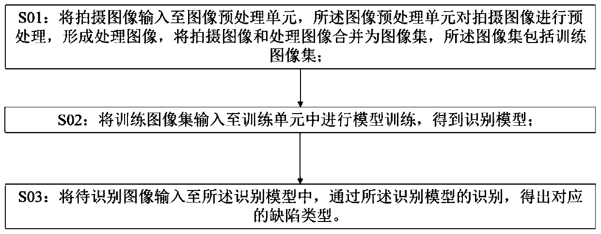
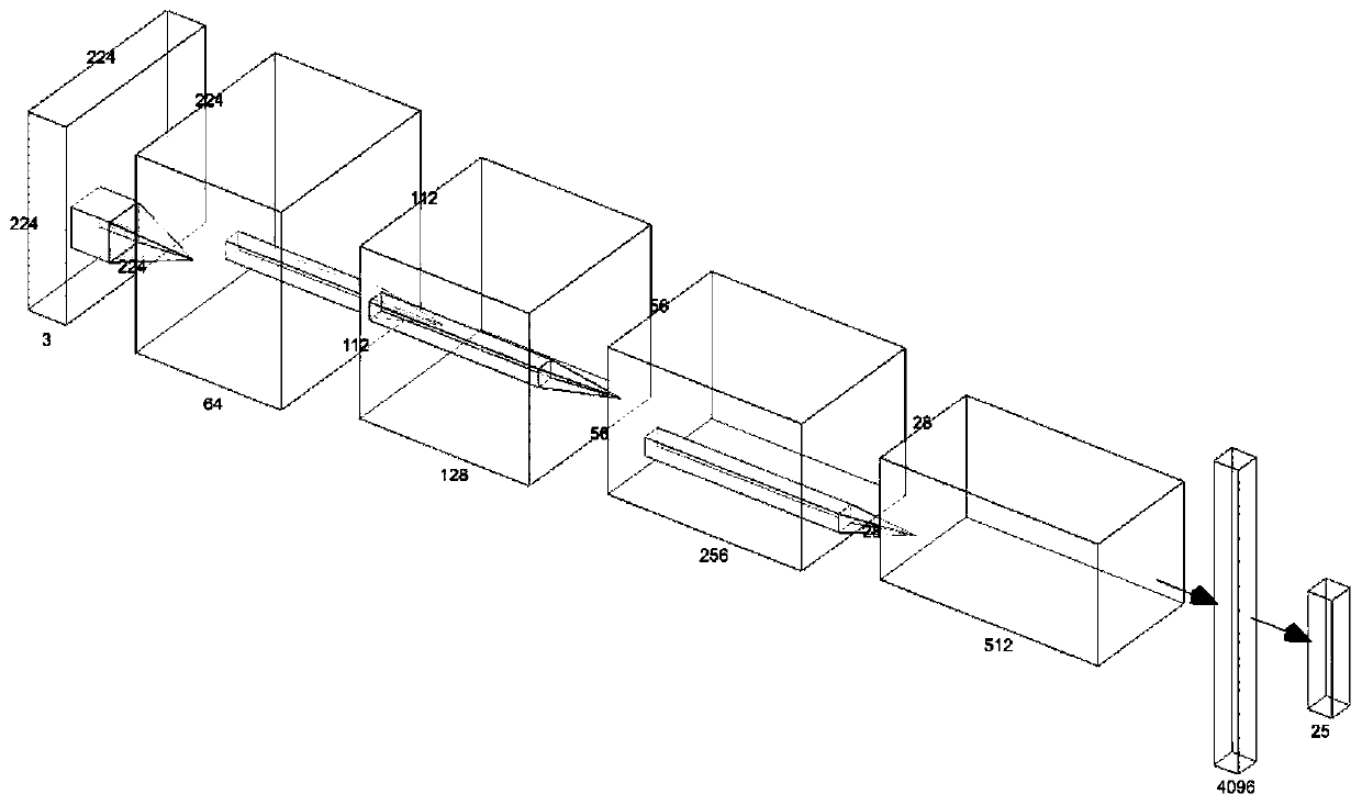
[0056] In the present invention, the identification model can be a deep convolutional neural network model, and its specific training steps are:
[0057] Step 1: Set the training image size in the training image set to 3 channels 224×224; in this embodiment, it can also be set to 1 channel image, and the channel size can be any value between 0-256;
[0058] Step 2: Input the training image to the input layer of the deep convolutional neural network model, and the size of the input layer of the deep convolutional neural network model is 224×224×3;
[0059] Step 3: The training image output from the input layer of the deep convolutional neural network model is input to the first convolutional layer C1 of the deep convolutional neural network model; the size of the first convolutional layer C1 of the deep convolutional neural network model is 224×224 ×64, using ReLU as the activation function; in this embodiment, the size of the sliding matrix can also be other values such as 3...
PUM
 Abstract
Description
Claims
Application Information