

VCSEL device for realizing polarization control and preparation method thereof
A polarization control and device technology, which is applied to laser components, lasers, electrical components, etc., can solve the problems of increasing device manufacturing costs and reducing energy conversion efficiency
- Summary
- Abstract
- Description
- Claims
- Application Information
AI Technical Summary
Problems solved by technology
Method used
Image

Examples
Embodiment 1
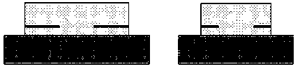
[0030] Embodiments of the present invention provide a VCSEL device and a manufacturing method thereof, such as figure 1 As shown, in this embodiment, the DBR high-aluminum component layer and the target oxide layer are etched and oxidized in different polarization directions to achieve structures with different oxidation lengths in different directions, so as to realize the two polarization directions of the VCSEL device. The effect of light control. The oxidation length refers to the inward oxidation length of the target oxide layer during the oxidation process. The device preparation method is as follows:
[0031] Step 1: Etching both sides of the epitaxial layer of the VCSEL device in the first direction to form two first channels, and oxidize from the first channel to the inside of the epitaxial layer to form a first oxide layer, and the oxidation time is X;
[0032] Step 2: Etching both sides of the epitaxial layer of the VCSEL device in the second direction to form two...
Embodiment 2
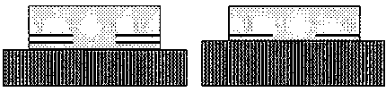
[0036] Embodiments of the present invention provide a VCSEL device and a manufacturing method thereof, such as figure 1 As shown, in this embodiment, the DBR high-aluminum component layer and the target oxide layer are etched and oxidized in different polarization directions to achieve structures with different oxidation lengths in different directions, so as to realize the two polarization directions of the VCSEL device. The effect of light control, the device preparation method is as follows:
[0037] Step 1: Etch both sides of the epitaxial layer of the VCSEL device in the first direction to form two first channels, and oxidize from the first channel to the inside of the epitaxial layer to form a first oxide layer on the sidewall of the first channel Protected by dielectric;
[0038] Step 2: Etching both sides of the epitaxial layer of the VCSEL device in the second direction to form two second channels, the mesa structure of the VCSEL device is defined by the first channe...
Embodiment 3
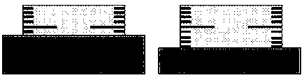
[0042] Embodiments of the present invention provide a VCSEL device and a manufacturing method thereof, such as figure 2 As shown, in this embodiment, the DBR high-aluminum component layer and the target oxide layer are etched and oxidized in different polarization directions to achieve a structure with different numbers of oxide layers in different directions, so as to achieve two polarizations of the VCSEL device. The effect of controlling the direction of light, the device preparation method is as follows:
[0043]Step 1: The epitaxial layer of the VCSEL device includes two or more target oxide layers, and the target oxide layers are separated by a stopper layer. The depth of the channel etch can be controlled by the stopper layer and the time of channel etching. The depth of the trench etch is used to control the amount of exposed sidewalls of the target oxide. Etching both sides of the first direction of the epitaxial layer of the VCSEL device forms two first trenches; t...
PUM
 Abstract
Description
Claims
Application Information