Display device and method of making the same

A technology of a display device and a manufacturing method, which can be applied to semiconductor devices, electrical components, circuits, etc., and can solve problems such as screen differences

Active Publication Date: 2022-08-09
BOE TECH GRP CO LTD +1
View PDF14 Cites 0 Cited by
  • Summary
  • Abstract
  • Description
  • Claims
  • Application Information

AI Technical Summary

Problems solved by technology

[0003] The present invention at least partly solves the problem that the existing display devices with multiple display screens have different screens after being used for a period of time, and provides a display that reduces the differences in the screens of different display screens of the same display device. Method of making the device

Method used


Image

  • Display device and method of making the same
  • Display device and method of making the same
  • Display device and method of making the same

Examples


Embodiment 1

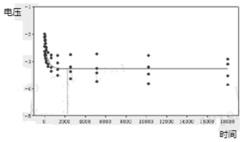
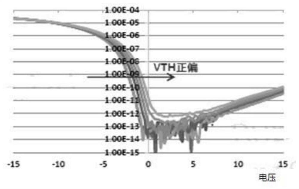
[0028] like Figure 1 to Figure 8 As shown, this embodiment provides a manufacturing method of a display device, including:

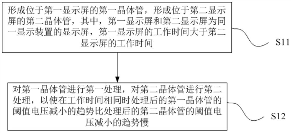
[0029] S11, forming a first transistor located at the first display screen, and forming a second transistor located at the second display screen, wherein the first display screen and the second display screen are the display screens of the same display device, and the working time of the first display screen greater than the working time of the second display.

[0030] S12. Perform the first processing on the first transistor, and perform the second processing on the second transistor, so that the threshold voltage of the processed first transistor decreases more than the threshold voltage of the processed second transistor when the operating time is the same The decreasing trend is slow.

[0031] It should be noted that the display device is mainly aimed at a display device with two display screens at the same time, that is, since the display device ...

Embodiment 2

[0035] like Figure 1 to Figure 8 As shown, this embodiment provides a manufacturing method of a display device, including:

[0036] S11, forming a first transistor located at the first display screen, and forming a second transistor located at the second display screen, wherein the first display screen and the second display screen are the display screens of the same display device, and the working time of the first display screen greater than the working time of the second display.

[0037] Preferably, the first display screen is a main display screen of the display device, and the second display screen is a sub-display screen of the display device.

[0038] That is to say, when the user uses the display device, the first display screen is used with a high frequency, and the second display screen is used with a low frequency, so that the use time of the first display screen is longer than that of the second display screen. .

[0039] S12. Perform the first processing on t...


PUM


Abstract

The present invention provides a display device and a manufacturing method thereof, belonging to the field of display technology, which can at least partially solve the problem that the existing display devices with multiple display screens have different images after a period of use. A manufacturing method of a display device of the present invention includes: forming a first transistor located on a first display screen, and forming a second transistor located on a second display screen, wherein the first display screen and the second display screen are the same display device The working time of the first display screen is longer than that of the second display screen; the first processing is performed on the first transistor, and the second processing is performed on the second transistor, so that when the working hours are the same, the processed first The decreasing trend of the threshold voltage of the transistor is slower than the decreasing trend of the threshold voltage of the processed second transistor.

Description

technical field [0001] The invention belongs to the field of display technology, and in particular relates to a display device and a manufacturing method thereof. Background technique [0002] With the development of science and technology, the existing display device is provided with at least two display screens, including a main display screen and a sub-display screen. The display time of the screen is relatively short, which may cause the aging degree of the transistors of the main display screen to be much greater than that of the transistors of the auxiliary display screen, resulting in differences in the picture quality of the main and auxiliary display screens, affecting the user experience. SUMMARY OF THE INVENTION [0003] The present invention at least partially solves the problem that the existing display devices with multiple display screens have different pictures after a period of use, and provides a display device that reduces the picture differences between...

Claims


Application Information

Patent Timeline
Patent Type & Authority Patents(China)
IPC IPC(8): H01L27/32
CPCH10K59/1213H10K59/12
Inventor 黄强马群何传友郝瑞杨光辉
Owner BOE TECH GRP CO LTD
Why Eureka
Try Eureka