Active matrix substrate and display device
An active matrix and display device technology, applied in the field of active matrix substrates and display devices, can solve problems such as display quality degradation, and achieve the effect of reducing display quality degradation
- Summary
- Abstract
- Description
- Claims
- Application Information
AI Technical Summary
Problems solved by technology
Method used
Image
Examples
Embodiment approach 1
[0033] Hereinafter, one embodiment of the present invention will be described in detail with reference to the drawings.
[0034] (watch)
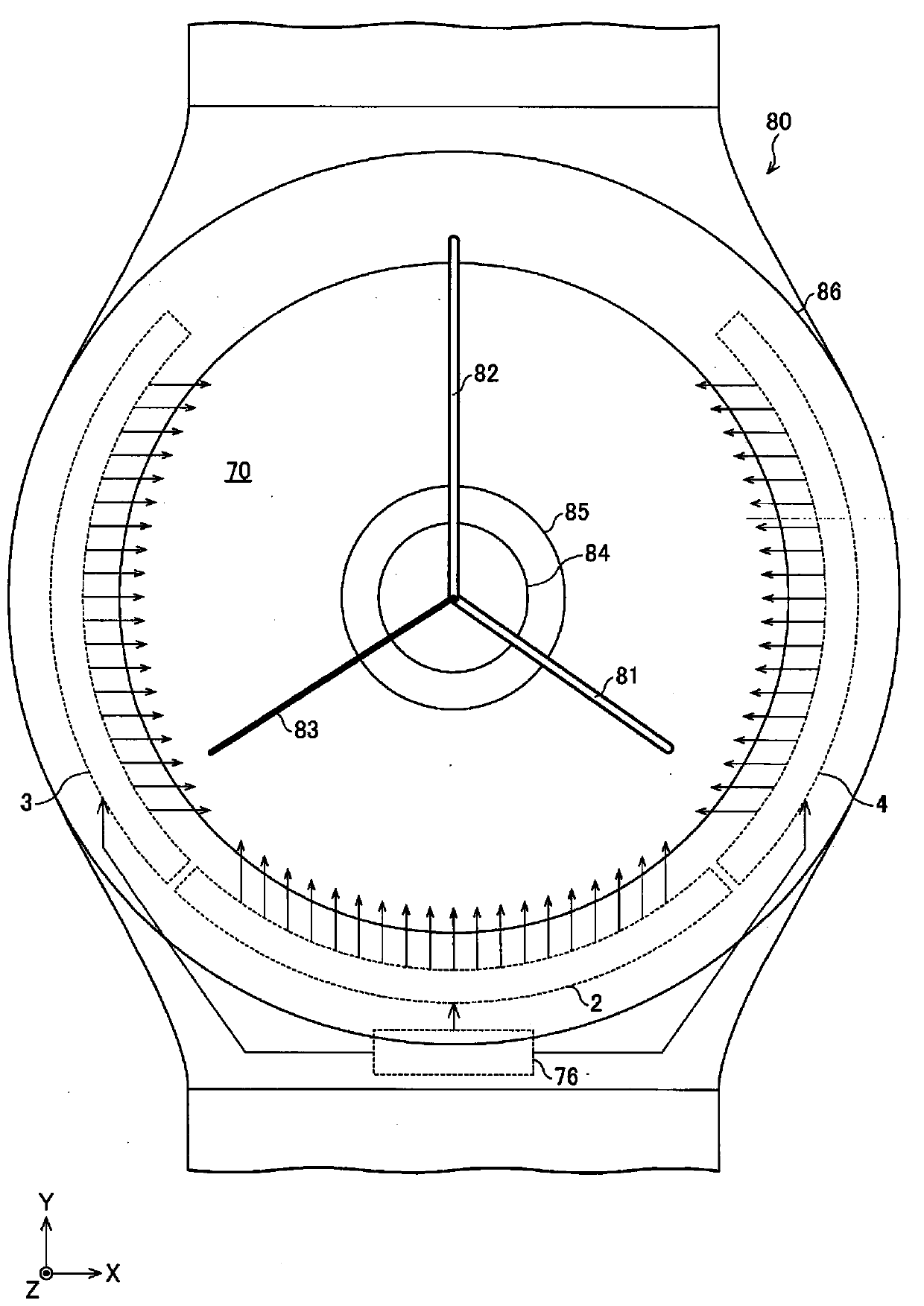
[0035] figure 1 It is a plan view showing a schematic configuration of a wristwatch 80 including a liquid crystal display panel 70 (display device) according to Embodiment 1 of the present invention.
[0036] Such as figure 1 As shown, a wristwatch 80 is an analog clock that displays time by rotating an hour hand 81 , a minute hand 82 , and a second hand 83 around a drive shaft 84 , and uses a liquid crystal display panel 70 for its dial. The driving shaft 84 passes through the opening 64 of the liquid crystal display panel 70 and is coupled to a mechanical driving mechanism built in the back of the liquid crystal display panel 70 . In addition, the liquid crystal display panel 70 is connected to the source driver 2 , the odd-numbered gate driver 3 and the even-numbered gate driver 4 , and the control circuit 76 built in the wristwatch...
Embodiment approach 2
[0221] Below, based on Figure 10 and Figure 11 Another embodiment of the present invention will be described. In addition, for convenience of description, members having the same functions as those described in the above-mentioned embodiments are denoted by the same reference numerals, and description thereof will be omitted.
[0222] Figure 10 It is a plan view showing a schematic configuration of an active matrix substrate 1' according to Embodiment 2. For convenience of illustration, the illustration of the gate line GL passing through the inner non-display area 12, the pixel electrode 50, etc. is omitted.
[0223] Such as Figure 10 As shown, like the active matrix substrate 1 of the first embodiment described above, the active matrix substrate 1' of the second embodiment includes: an insulating substrate 10, 2M gate lines GL, and 12N roots intersecting the gate lines GL. The pole line SL, the pixel transistor 40 corresponding to the intersection of the gate line G...
PUM
 Abstract
Description
Claims
Application Information


