Pixel circuit and driving method thereof, array substrate and display device

A pixel circuit and circuit technology, applied in static indicators, instruments, etc., can solve the problems of poor appearance of the display screen, poor line, different power supply voltage drop, etc.

Pending Publication Date: 2020-04-24
BOE TECH GRP CO LTD +1
View PDF10 Cites 8 Cited by
  • Summary
  • Abstract
  • Description
  • Claims
  • Application Information

AI Technical Summary

Problems solved by technology

[0003] Although OLED has many advantages, the threshold voltage of the driving transistor at different positions will be different due to process deviation in the manufacturing process of its driving transistor.
And as the working time is extended and the use environment changes, the threshold voltage of the drive transistor will drift
At the same time, the different positions of each pixel will cause the voltage drop (IRDrop) of the power supply to be different, which will affect the current driving the OLED.
If the threshold voltage and power supply IR drop cannot be compensated, it will lead to uneven light

Method used


Image

  • Pixel circuit and driving method thereof, array substrate and display device
  • Pixel circuit and driving method thereof, array substrate and display device
  • Pixel circuit and driving method thereof, array substrate and display device

Examples


example 1

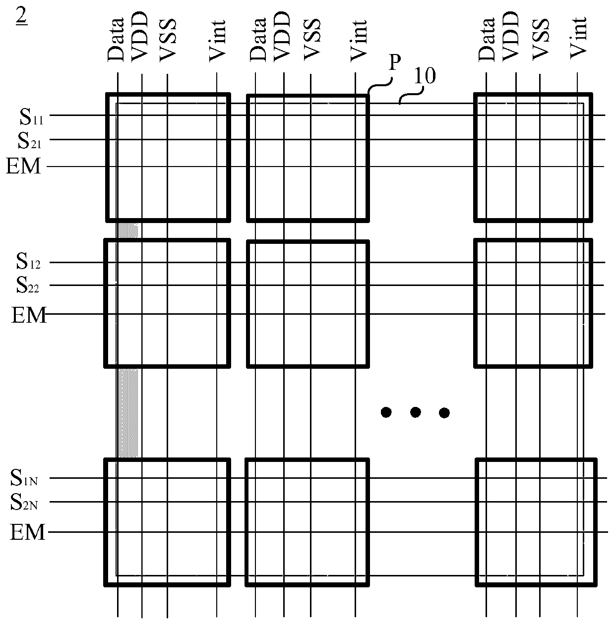
[0073] Example 1, the first sub-pixel is located in the first column of the first row, the second sub-pixel is located in the second column of the first row, and the third sub-pixel is located in the first column of the second row; Example 2, the first sub-pixel is located in the first row In the first column, the second sub-pixel is located in the second column of the first row, and the third sub-pixel is located in the second column of the second row; Example 3, the first sub-pixel is located in the first column of the first row, and the second sub-pixel is located in the second column The first column of the first row, the third sub-pixel is located in the second column of the first row; Example 4, the first sub-pixel is located in the first column of the first row, the second sub-pixel is located in the first column of the second row, and the third sub-pixel is located in the first column Two rows and two columns.

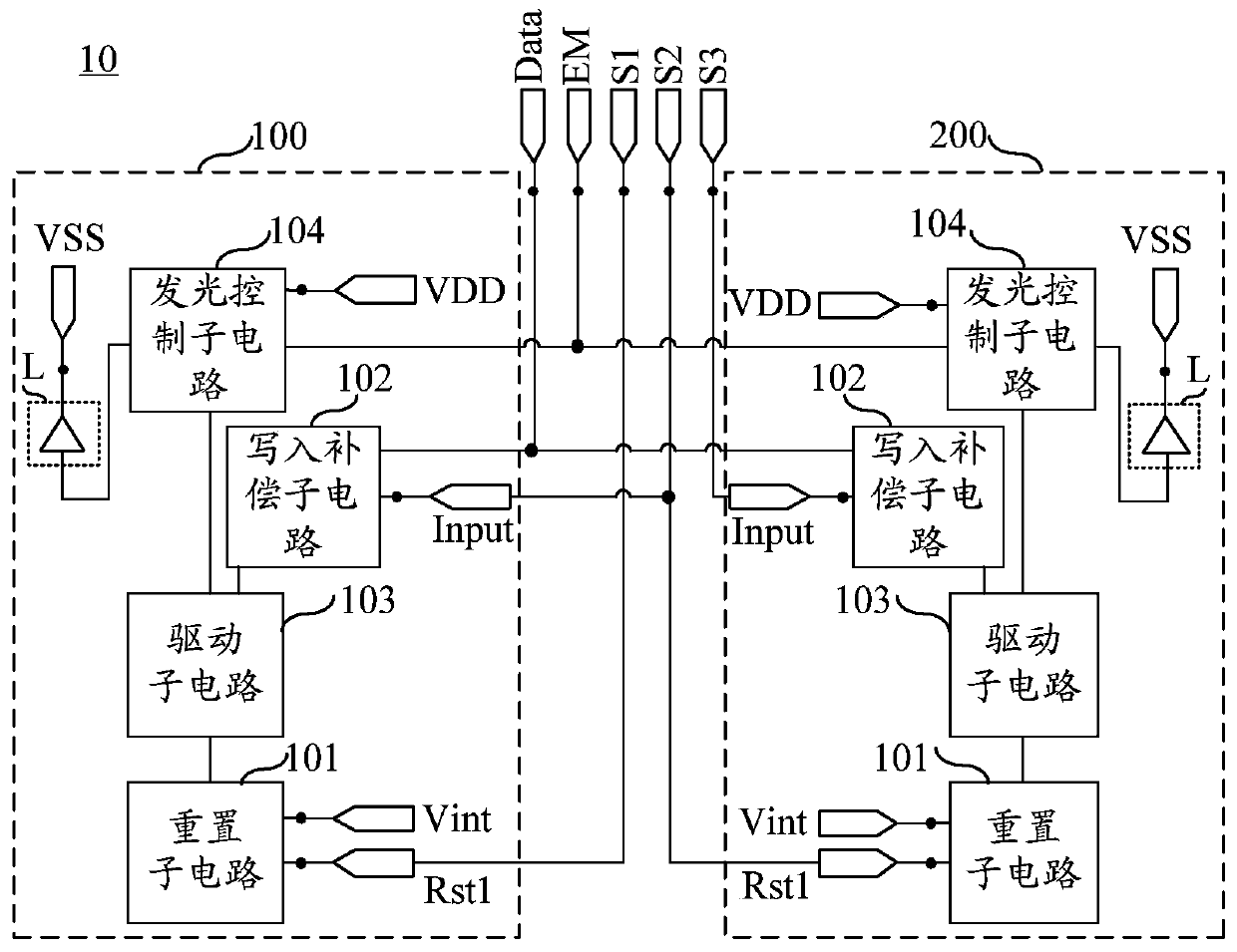
[0074] Here, the circuit structures of the first sub-pixe...


PUM


Abstract

The embodiment of the invention provides a pixel circuit and a driving method thereof, an array substrate and a display device, relates to the technical field of display, and can improve the display effect. The pixel circuit comprises a first sub-pixel circuit and a second sub-pixel circuit, each of the first sub-pixel circuit and the second sub-pixel circuit comprises a reset sub-circuit, a write-in compensation sub-circuit, a driving sub-circuit, a light-emitting control sub-circuit and a light-emitting device; the reset sub-circuit is configured to input the voltage provided by the initialvoltage end to the driving sub-circuit under the control of the first reset control end; the write-in compensation sub-circuit is configured to write a signal output by the data end into the driving sub-circuit under the control of the write-in control end so as to perform threshold voltage compensation on the driving sub-circuit; and the light-emitting control sub-circuit is configured to conducta current path between the first power supply voltage end and the second power supply voltage end under the control of the enabling end, and transmit the driving current provided by the driving sub-circuit to the light-emitting device.

Description

technical field [0001] The present invention relates to the field of display technology, in particular to a pixel circuit and a driving method thereof, an array substrate and a display device. Background technique [0002] Organic light emitting diode (Organic Light Emitting Diode, OLED) display device is one of the hotspots in the current research field. OLED has the advantages of low energy consumption, low production cost, self-illumination, wide viewing angle and fast response speed. [0003] Although the OLED has many advantages, the threshold voltages of the driving transistors at different positions are different due to process deviations during the manufacturing process of the driving transistors. And as the working time is extended and the use environment changes, the threshold voltage of the driving transistor will drift. At the same time, the different positions of the pixels will lead to different voltage drops (IRDrop) of the power supply, which will affect the...

Claims


Application Information

Patent Timeline
IPC IPC(8): G09G3/3208
CPCG09G3/3208G09G2300/0804G09G2310/061G09G2320/045G09G2300/0408G09G2310/0251G09G3/3241G09G3/3233G09G2300/0426G09G2300/0819G09G2300/0842G09G2300/0861G09G2310/08G09G3/3258G09G2320/043G09G3/325
Inventor 张陶然周炟廖文骏莫再隆
Owner BOE TECH GRP CO LTD
Why Eureka
Try Eureka