Edge defect inspection method

An inspection method and edge defect technology, applied in the field of inspection, can solve problems such as failure of protective structure or undetected cracks, distortion of grain edge search, undetected cracks of protective structure, etc.

Active Publication Date: 2020-05-05
CHIPMOS TECH INC
View PDF11 Cites 0 Cited by
  • Summary
  • Abstract
  • Description
  • Claims
  • Application Information

AI Technical Summary

Problems solved by technology

However, since the difference in the gray scale value of the image depends on the adjustment of the light source, the light source decay period and the reflection degree of the product surface, these uncertain factors can easily cause the search distortion of the grain edge
In the case where the grain edge has been distorted, when judging from the grain edge with a fixed grain chipping parameter specification, it may happen that the chipping or crack that actually damaged the protective structure is not detected
In addition, when the wafer cutting is offset, the distance from the four sides of the die to the protection structure will be different. Checking in the above-mentioned way, it may happen that the protection structure has actually been damaged on one or some sides. Structural breakage or cracks are not detected

Method used


Image

  • Edge defect inspection method
  • Edge defect inspection method
  • Edge defect inspection method

Examples


Embodiment Construction

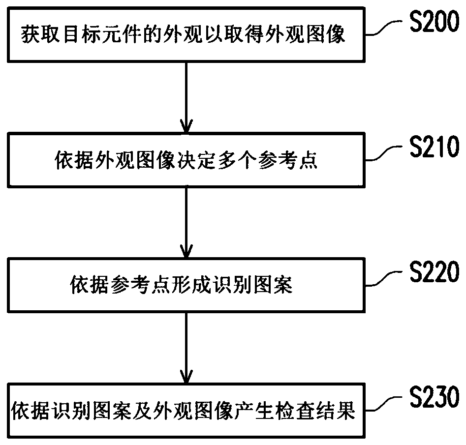
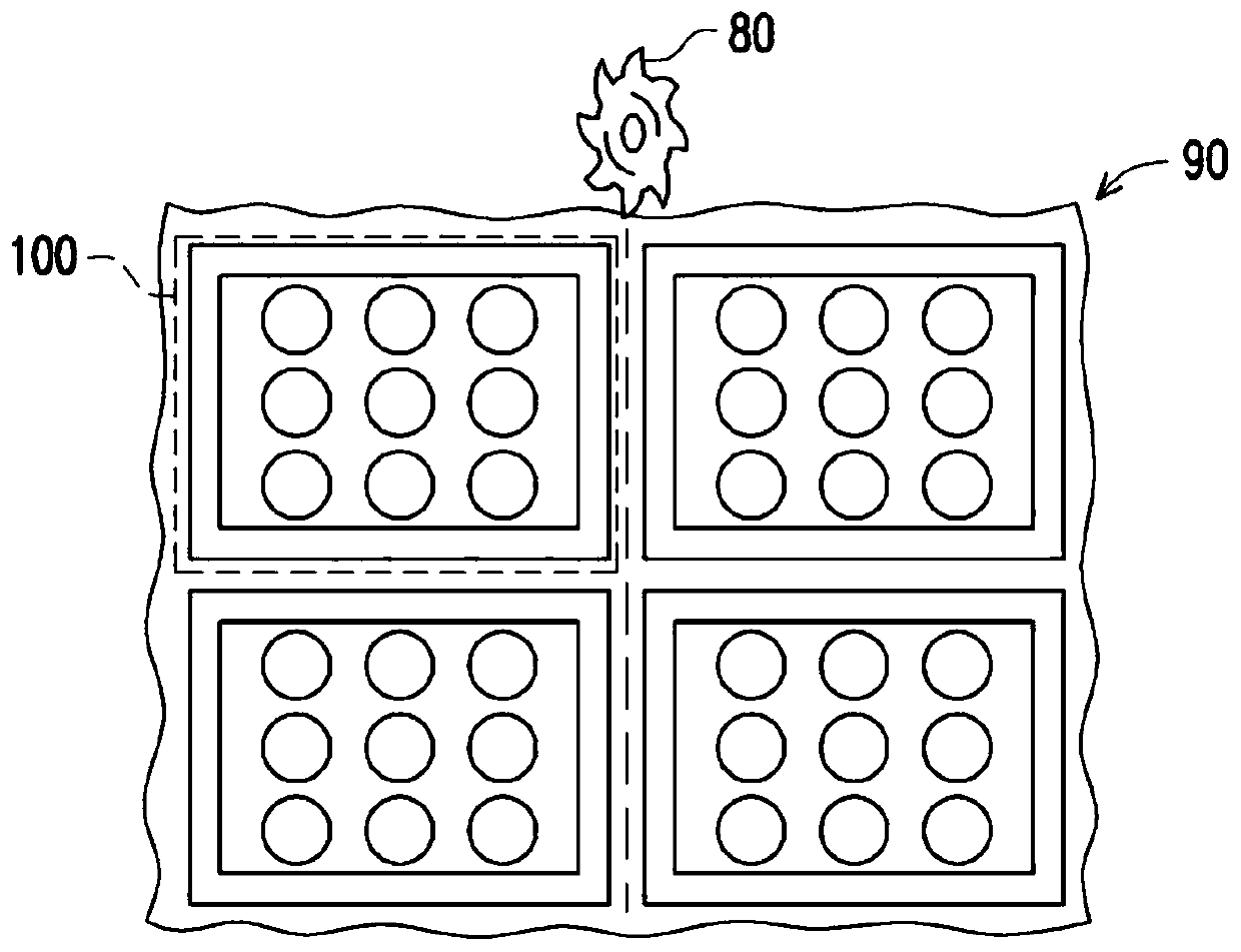
[0036] figure 1 It is a flow chart of steps of an edge defect inspection method according to an embodiment of the present invention. figure 2 It is a schematic diagram of cutting out target elements in an embodiment of the present invention. Please refer to figure 1 and figure 2 . The present embodiment provides an edge defect inspection method, and the edge defect inspection method is suitable for inspecting a target device 100 , such as a die or a WLC package separated from a wafer dicing unit. In this embodiment, the target component 100 is a wafer-level chip package cut out of a wafer 90 by the dicing device 80, such as figure 2 shown, but the present invention is not limited thereto.

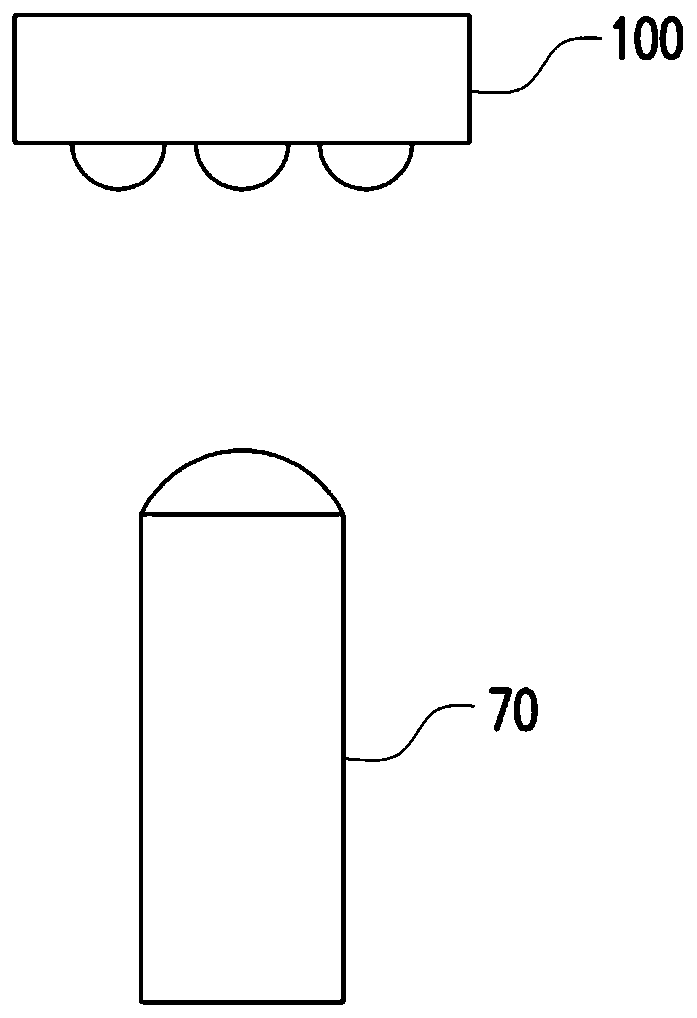
[0037] image 3 It is a schematic diagram of the appearance of the acquired target element in an embodiment of the present invention. Figure 4A to Figure 4D It is a top view of an edge defect inspection method of a target component in an embodiment of the present invention. Plea...


PUM


Abstract

The invention provides an edge defect inspection method. The edge defect inspection method comprises the following steps: acquiring the appearance of a target element to acquire an appearance image; determining a plurality of reference points according to the appearance image; forming an identification pattern according to the reference point; and generating an inspection result according to the identification pattern and the appearance image.

Description

technical field [0001] The present invention relates to an inspection method, and in particular to an edge defect inspection method. Background technique [0002] In the semiconductor industry, after the integrated circuit is produced on the wafer, it needs to be manufactured through chip packaging to prevent the integrated circuit from being polluted by the outside world, and to form an electrical connection path between the chip and the electronic system. There are two commonly used chip packaging methods: one is to cut the processed wafer into multiple dies, and then carry out subsequent packaging and manufacturing; the other is wafer-level packaging, that is, packaging directly on the entire chip After fabrication, the wafer is diced to form multiple individual chip packages. However, edge defects such as chipping or cracks may occur at the edge of the die / chip no matter the singulated die or WLC package after dicing. Therefore, it is necessary to select defective die ...

Claims


Application Information

Patent Timeline
Patent Type & Authority Applications(China)
IPC IPC(8): H01L21/66
CPCH01L22/12H01L22/20
Inventor 杨丰瑞张哲恺李忠儒林振斌林尚德刘宗祐
Owner CHIPMOS TECH INC
Why Eureka
Try Eureka