Supercharge Your Innovation With Domain-Expert AI Agents!

Buffer circuit and crystal oscillator circuit

A buffer circuit, crystal oscillator circuit technology, applied in the direction of logic circuit, logic circuit connection/interface layout, logic circuit coupling/interface using field effect transistors, etc., can solve problems such as output clock abnormality, and achieve noise and dynamic ESD interference suppression Effect

Pending Publication Date: 2020-05-08
HI TREND TECH SHANGHAI
View PDF5 Cites 0 Cited by
  • Summary
  • Abstract
  • Description
  • Claims
  • Application Information

AI Technical Summary

Problems solved by technology

[0003] In view of the shortcomings of the prior art described above, the purpose of the present invention is to provide a buffer circuit and a crystal oscillator circuit, which are used to solve the problem that the output of the existing crystal oscillator circuit is affected by noise or dynamic ESD interference. abnormal clock problem

Method used


Image

  • Buffer circuit and crystal oscillator circuit
  • Buffer circuit and crystal oscillator circuit
  • Buffer circuit and crystal oscillator circuit

Examples


Embodiment

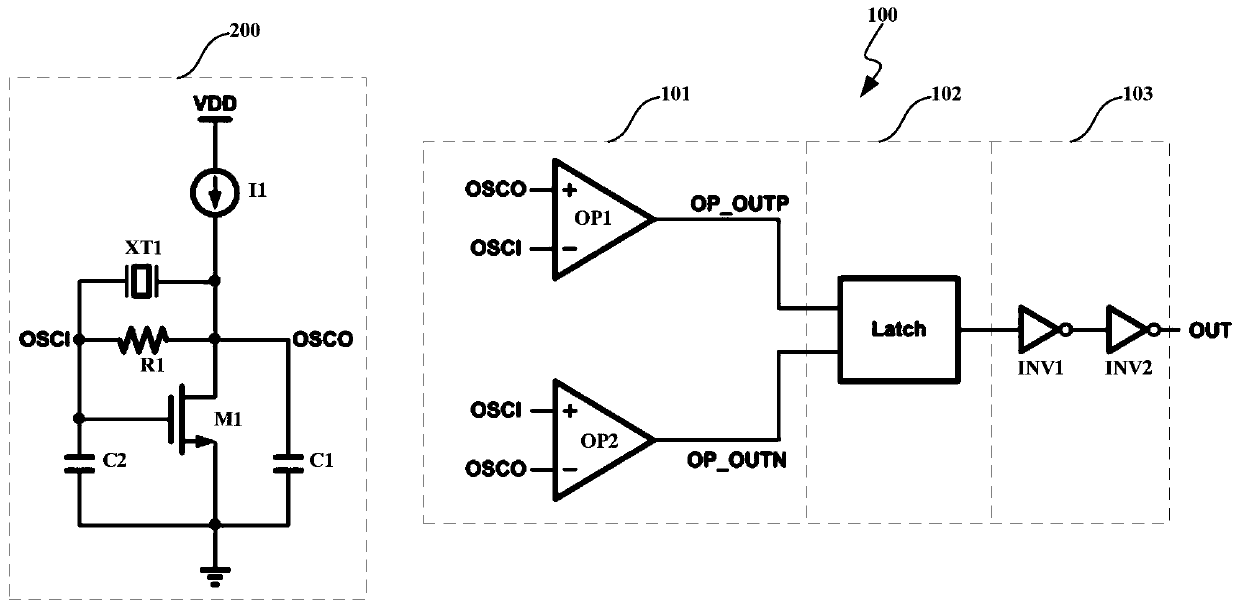
[0030] like figure 1 As shown, this embodiment provides a buffer circuit, and the buffer circuit 100 includes:

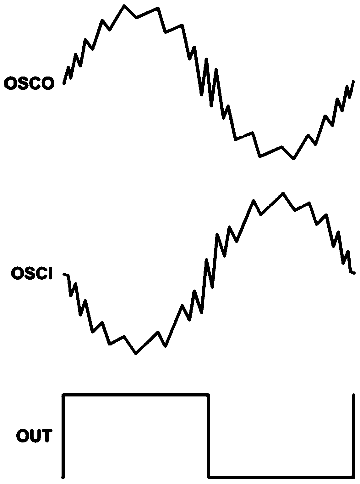
[0031] The differential amplification unit 101 is configured to differentially amplify the input oscillation signal OSCI and the output oscillation signal OSCO of the crystal oscillator to generate a set of differential signals;

[0032] A swing amplifying unit 102, connected to the differential amplifying unit 101, configured to amplify the swing of a set of differential signals output by the differential amplifying unit 101 to generate a full-rail signal;

[0033] The output unit 103 is connected to the swing amplifying unit 102 and configured to invert the full-rail signal output by the swing amplifying unit 102 to generate a clock signal.

[0034] As an example, such as figure 1 As shown, the differential amplification unit 101 includes: a first operational amplifier OP1 and a second operational amplifier OP2, wherein the non-inverting input terminal of the fi...


PUM


Abstract

The invention provides a buffer circuit and a crystal oscillator circuit, and the buffer circuit comprises a differential amplification unit which is used for carrying out the differential amplification of an input oscillation signal and an output oscillation signal of a crystal oscillator, so as to generate a group of differential signals; a swing amplification unit which is connected to the differential amplification unit and is used for carrying out swing amplification on the group of differential signals output by the differential amplification unit so as to generate a full-swing signal; an output unit which is connected to the swing amplification unit and is used for inverting the full-swing signal output by the swing amplification unit to generate a clock signal. Via the buffer circuit and the crystal oscillator circuit disclosed in the invention, the problem that the output clock is abnormal when the power supply and the ground of the existing crystal oscillator circuit are influenced by noise or dynamic ESD interference to generate large fluctuation is solved.

Description

technical field [0001] The invention relates to the field of integrated circuit design, in particular to a buffer circuit and a crystal oscillator circuit. Background technique [0002] In the traditional Pierce crystal oscillator circuit, after the crystal oscillator completes the start-up, the amplitude of its input and output oscillation signals is generally stable in the order of several hundred mV; however, when the power supply and ground are affected by noise or dynamic ESD interference, large fluctuations occur At this time, since the amplitude of the oscillation waveform of the input oscillation signal and output oscillation signal of the crystal oscillator is small, noise or interference will have a greater impact on it, which will easily lead to abnormal output clocks. Contents of the invention [0003] In view of the shortcomings of the prior art described above, the purpose of the present invention is to provide a buffer circuit and a crystal oscillator circui...

Claims


Application Information

Patent Timeline
Patent Type & Authority Applications(China)
IPC IPC(8): H03K19/0185
CPCH03K19/018507
Inventor 程龙马侠
Owner HI TREND TECH SHANGHAI
Features
  • R&D
  • Intellectual Property
  • Life Sciences
  • Materials
  • Tech Scout
  • Unparalleled Data Quality
  • Higher Quality Content
  • 60% Fewer Hallucinations
Learn More