Detection device and method for simultaneous equal-optical-path imaging and equal-illuminance illumination of double sides of crystal grain based on image-combining optical element

A technology for optical components and detection devices, applied in optical components, measurement devices, optical testing flaws/defects, etc., can solve problems such as affecting double-sided image recognition and imaging quality, increasing the complexity of mechanical structures, and breaking edges and corners. To achieve the effect of easy and convenient debugging, high precision of double-sided imaging, and simple assembly structure

Pending Publication Date: 2020-05-15
QUANZHOU NORMAL UNIV
View PDF1 Cites 13 Cited by
  • Summary
  • Abstract
  • Description
  • Claims
  • Application Information

AI Technical Summary

Problems solved by technology

[0002] The applicant's previous application, title: "Optical detection device and method for realizing equal optical path imaging of semiconductor crystal grains on both surfaces" application number: "2019113692573, in which the synthesis of the images on the opposite sides of the crystal grains in the CCD sensor requires two pieces based on Totally reflective right-angle reflective prisms (such as figure 1 shown), or a right-angle double-sided reflective prism (such as figure 2 shown); the former has high technical difficulty requirements for the precise assembly and debugging of right-angle reflective prisms, and the latter is not a priority option because of the need for high-reflective reflective coating and reliability, and the 45-degree prism Edges will inevitably have broken edges and corners during the processing process, and two adjacent defective edges will affect the recognition and imaging quality of the double-sided image. necessary
[0003] In addition, the applicant has previously applied for two patents, patent title: "Method for Obtaining Complete Isoluminance Illumination for Optical Detection on Opposite Two Sides of Semiconductor Die", Patent Application Number: "2019113692588"; A new method of illumination compensation for simultaneous detection of surface defects", patent application number: "201911315115.9, the double-sided imaging optical paths proposed by these two patent applications need to add specific illumination optical elements (optical wedge or right-angle Beam splitting prism) to obtain the purpose of double-sided imaging equal-illuminance illumination, such as image 3 , as shown in 4 and 5, image 3 The lighting source system requires an optical wedge, which increases the complexity of the mechanical structure; Figure 4 , The lighting source system of 5 needs a right-angle beam splitter prism and thus produces 50% light energy loss

Method used


Image

  • Detection device and method for simultaneous equal-optical-path imaging and equal-illuminance illumination of double sides of crystal grain based on image-combining optical element
  • Detection device and method for simultaneous equal-optical-path imaging and equal-illuminance illumination of double sides of crystal grain based on image-combining optical element
  • Detection device and method for simultaneous equal-optical-path imaging and equal-illuminance illumination of double sides of crystal grain based on image-combining optical element

Examples


Embodiment Construction

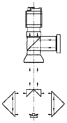
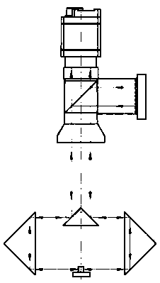
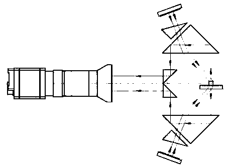
[0024] The present invention is based on the double-sided imaging optical element of the crystal grain with equal optical path imaging and equal illuminance illumination. The detection device includes a camera 1, a telecentric imaging lens 2, an imaging optical element 3 and a semiconductor crystal arranged in sequence in the direction of the vertical optical path. grain 4, the semiconductor crystal grain 4 can be placed on the stage 5, and the two sides between the image-combining optical element and the semiconductor grain are provided with a trapezoidal transfer prism 6, and the two sides 401 of the semiconductor grain are respectively Through the two trapezoidal relay prisms 6a, 6b, the image-combining optical element 3 forms images in different regions on the sensor surface of the camera 1 with dual optical paths.

[0025] Alternatively, the detection device of the present invention based on the double-sided simultaneous equal optical path imaging of the crystal grain of t...


PUM


Abstract

The invention discloses a detection device and method for simultaneous equal-optical-path imaging and equal-illuminance illumination of double sides of a crystal grain based on an image-combining optical element. The device comprises a camera, a telecentric imaging lens, an image-combining optical element and a semiconductor crystal grain which are sequentially arranged in the direction perpendicular to an optical path, trapezoidal image rotation prisms are arranged at two side parts between the image-combining optical element and the semiconductor crystal grain; and two side surfaces of the semiconductor crystal grain are imaged at different area positions on the surface of a camera sensor through the trapezoidal image rotation prisms and the image-combining optical element in a dual-optical-path manner. According to the invention, the single image-combining optical element is used for replacing two independent right-angle image rotation prisms to realize an image combining function of a double-sided imaging optical path, the scheme is simple in assembly structure, the image combining optical path is simpler and more convenient to debug, and the double-sided image combining precision is higher.

Description

Technical field: [0001] The invention belongs to the field of optical detection and machine vision, and in particular relates to a detection device and method for simultaneous equal optical path imaging and equal illuminance illumination on both sides of a crystal grain based on an imaging optical element. Background technique: [0002] The applicant's previous application, title: "Optical detection device and method for realizing equal optical path imaging of semiconductor crystal grains on both surfaces" application number: "2019113692573, in which the synthesis of the images on the opposite sides of the crystal grains in the CCD sensor requires two pieces based on Totally reflective right-angle reflective prisms (such as figure 1 shown), or a right-angle double-sided reflective prism (such as figure 2 shown); the former has high technical difficulty requirements for the precise assembly and debugging of right-angle reflective prisms, and the latter is not a priority opt...

Claims


Application Information

Patent Timeline
Patent Type & Authority Applications(China)
IPC IPC(8): G01N21/88G01N21/95G02B17/08
CPCG01N21/8806G01N21/9501G01N2021/8841G02B17/0856
Inventor 廖廷俤颜少彬段亚凡李世展
Owner QUANZHOU NORMAL UNIV
Why Eureka
Try Eureka