PCB board card signal line LOSS testing device

A PCB board and testing device technology, which is applied in the field of PCB card signal line LOSS testing device, can solve problems affecting test results, inaccurate data, etc., and achieve the effects of ensuring accuracy, improving applicability, and avoiding shaking

Inactive Publication Date: 2020-05-15
SUZHOU LANGCHAO INTELLIGENT TECH CO LTD
View PDF0 Cites 6 Cited by
  • Summary
  • Abstract
  • Description
  • Claims
  • Application Information

AI Technical Summary

Problems solved by technology

The contact strength between the probe and the PCB board has a great influence on the test results. If

Method used


Image

  • PCB board card signal line LOSS testing device
  • PCB board card signal line LOSS testing device
  • PCB board card signal line LOSS testing device

Examples


Embodiment Construction

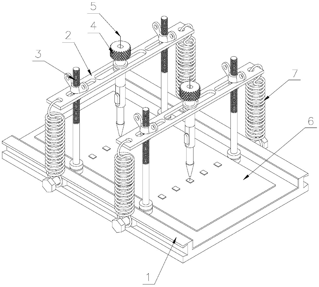
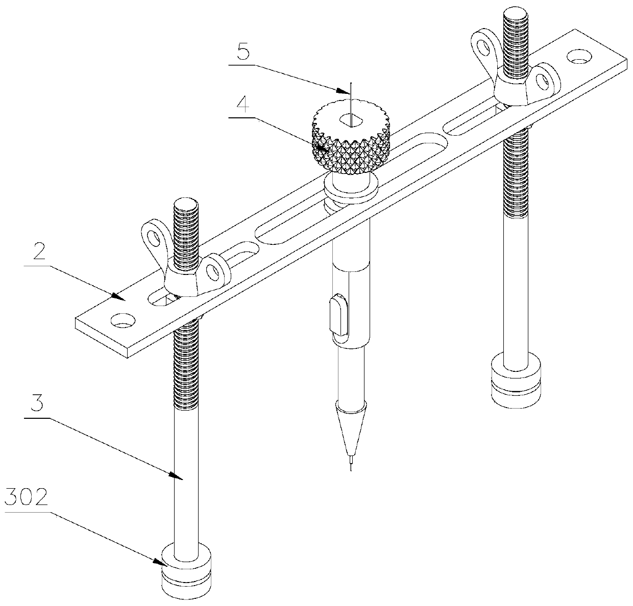
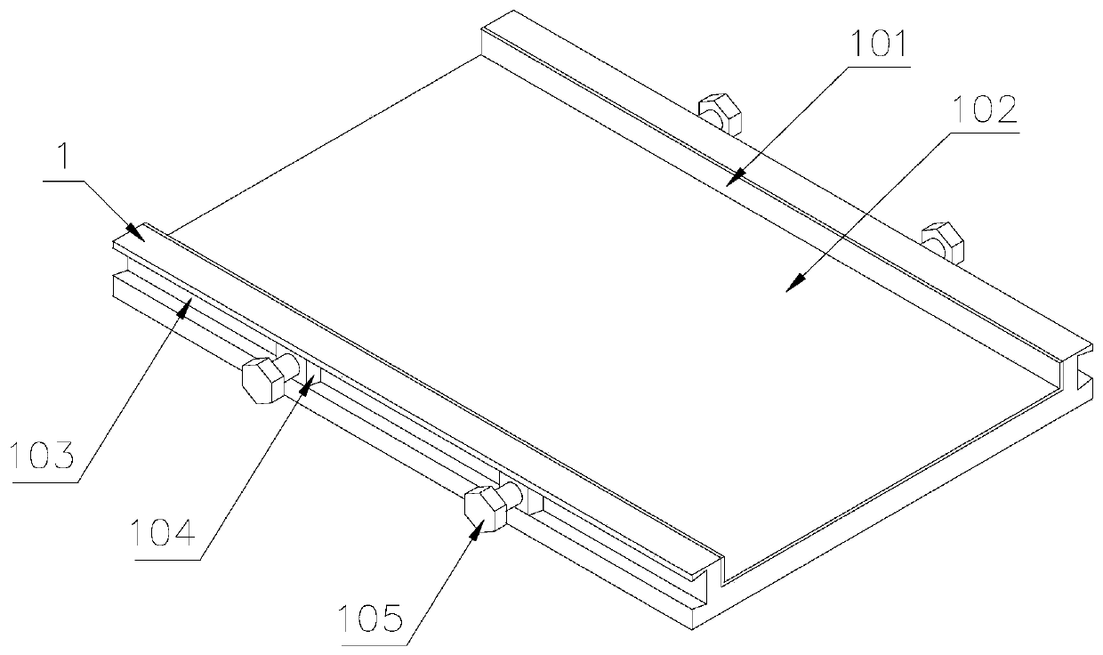
[0036] Attached below Figure 1-8 , clearly and completely describe the technical solutions in the embodiments of the present invention, obviously, the described embodiments are only some of the embodiments of the present invention, not all of them. Based on the embodiments of the present invention, all other embodiments obtained by persons of ordinary skill in the art without making creative efforts belong to the protection scope of the present invention.

[0037] In describing the present invention, it should be understood that the terms "longitudinal", "transverse", "upper", "lower", "front", "rear", "left", "right", "vertical", The orientations or positional relationships indicated by "horizontal", "top", "bottom", "inner", "outer", etc. are based on the orientations or positional relationships shown in the drawings, and are only for the convenience of describing the present invention, rather than indicating or It should not be construed as limiting the invention by imply...


PUM


Abstract

The invention discloses a PCB board card signal line LOSS testing device. The device comprises a base, a cross beam, clamping arms and a clamping device; a probe is arranged in the clamping device, the lower end of the probe extends out of the clamping device, the clamping device is installed on the cross beam, the clamping arms are distributed on the two sides of the clamping device, and the distance between the clamping arms on the two sides is equal to the width of a PCB card; the base is arranged at the lower part of the cross beam, and the PCB card is placed on the base; hanging holes areformed in the two ends of the cross beam, hanging rods corresponding to the hanging holes in position are arranged on the two sides of the base, tension springs are arranged on the hanging rods, oneends of the tension springs are hung on the hanging rods, and the other ends of the tension springs are hung in the hanging holes. The clamping device is arranged on the cross beam, the probe is installed in the clamping device, the clamping arms are arranged on the two sides of the clamping device, a PCB is clamped through the clamping arms, meanwhile, the probe is kept in contact with a test point of the PCB through the tension spring, and the accuracy of test data is guaranteed.

Description

technical field [0001] The invention belongs to the technical field of board card testing, in particular to a PCB board card signal line LOSS testing device. Background technique [0002] At present, the transmission rate of the signal line in the PCB board is getting higher and higher, so the loss (LOSS) parameter of the signal line of the board card is becoming more and more important. The loss reflects the quality of the transmission signal of the PCB board card, so R&D testers have higher and higher requirements for PCB board testing. Therefore, in the product design stage, controlling PCB loss is a very important link. PCB is the core of the server. Basically, in order to ensure the stable operation of the server, it is necessary to do a lot of tests on the PCB board to ensure the pass rate of the PCB. [0003] Now PNA (network analyzer, obtains S parameters, used for loss test of PCB board card) is a four-port network for testing loss, corresponding to four test point...

Claims


Application Information

Patent Timeline
IPC IPC(8): G01R31/28G01R1/04
CPCG01R1/0425G01R31/2801G01R31/2806G01R31/2808G01R31/281G01R31/2818
Inventor 刘安阳
Owner SUZHOU LANGCHAO INTELLIGENT TECH CO LTD
Why Eureka
Try Eureka