Product defect detection method, device and system
A technology for product defect and defect detection, applied in image analysis, image enhancement, instruments, etc., can solve the problems of fluctuation of inspection quality, high labor intensity of human inspection, and shortage of human resources, and achieve the effect of improving accuracy
- Summary
- Abstract
- Description
- Claims
- Application Information
AI Technical Summary
Problems solved by technology
Method used
Image
Examples
Embodiment 1
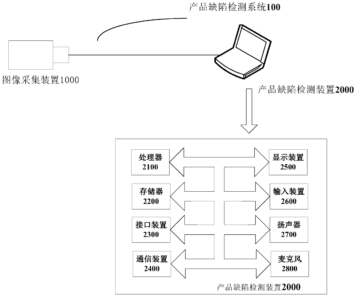
[0030] figure 1 is a block diagram of the hardware configuration of the product defect detection system 100 according to the embodiment of the present invention.
[0031] Such as figure 1 As shown, the product defect detection system 100 includes an image acquisition device 1000 and a product defect detection device 2000 .
[0032] The image capture device 1000 is used to capture product images, and provide the captured product images to the product defect detection device 2000 .
[0033] The image acquisition device 1000 may be any imaging device capable of taking pictures, such as a camera.
[0034] The product defect detection device 2000 can be any electronic equipment, such as PC, notebook computer, server and so on.
[0035] In this example, refer to figure 1 As shown, the product defect detection device 2000 may include a processor 2100, a memory 2200, an interface device 2300, a communication device 2400, a display device 2500, an input device 2600, a speaker 2700,...
Embodiment 2
[0042] In the process of product manufacturing, factors such as unstable process, insufficient mechanical positioning accuracy, and the environment in the factory building often cause the produced products to have various forms of defects or defects. In the early stage of product manufacturing, there are often very few bad samples, and classification algorithms based on big data and big models are difficult to meet the requirements of the production line.
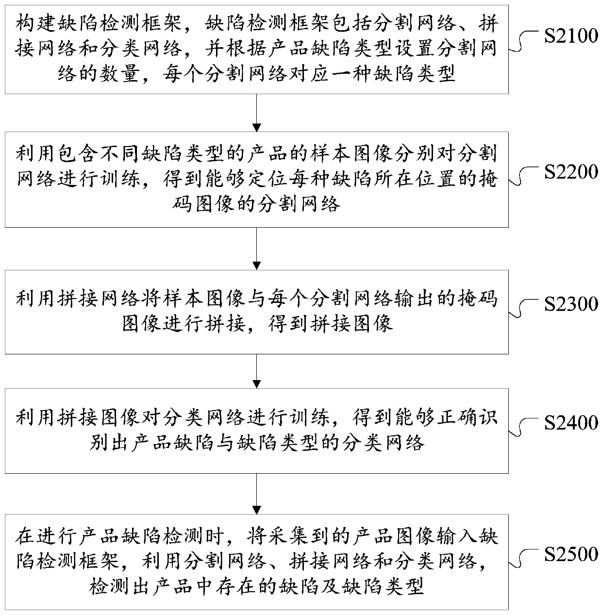
[0043]In view of the above-mentioned small sample problem, the embodiment of the present application first uses the image segmentation algorithm to predict possible defects and their positions in the image, and generates a corresponding mask (mask) image, and then stitches the original image and the mask image, and inputs classifiers to classify different defects.
[0044] figure 2 The flow chart of the product defect detection method shown in the embodiment of the present invention, such as figure 2 As shown, the metho...
Embodiment 3
[0060] The embodiment of the present application also provides a product defect detection method. In this embodiment, in the above step S2200, using sample images of products containing different defect types to train the segmentation network respectively includes S2210-S2220:
[0061] S2210. Input multiple sample images containing different defect types to multiple segmentation networks respectively.
[0062] In this embodiment, one sample image may contain n defect types, or may contain less than n defect types, and the defect types contained in each sample image may be the same or different.
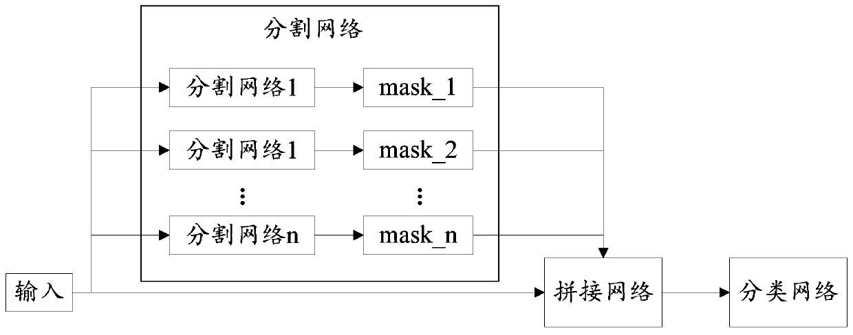
[0063] refer to image 3 , image 3 It shows that sample images containing n types of defects are input to n segmentation networks, and the n types of defects are all defects that can be segmented and located using segmentation algorithms, and each segmentation network outputs a mask image for locating the position of the defect, which is image 3 The mask images mask_1, mask_2, ....
PUM
 Abstract
Description
Claims
Application Information


