
Method for forming contact groove and semiconductor

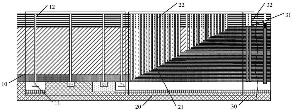
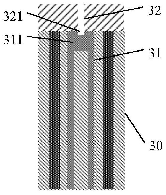
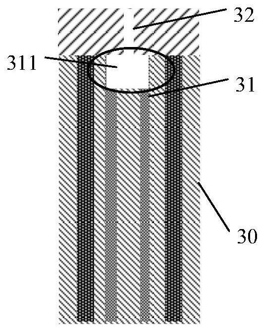
A semiconductor and contact layer technology, which is applied to the contact groove formation method and the semiconductor field, can solve the problems of increased time consumption, high cost, and long etching time of contact point through holes, and achieves cost reduction and time consumption, and increased etching. Corrosion time, the effect of ensuring electrical consistency

Active Publication Date: 2021-07-20
YANGTZE MEMORY TECH CO LTD
View PDF6 Cites 0 Cited by
  • Summary
  • Abstract
  • Description
  • Claims
  • Application Information

AI Technical Summary

Problems solved by technology

However, the cost of photolithography and etching for contact vias in different areas is still high
In addition, with the increase in the number of stacked layers, the etching time of the contact via holes is getting longer and longer, and the exposure and etching of the contact via holes will also bring a huge time-consuming increase.

Method used


Image

  • Method for forming contact groove and semiconductor
  • Method for forming contact groove and semiconductor
  • Method for forming contact groove and semiconductor

Examples


Embodiment Construction

[0033] In order to make the purpose, technical solution and advantages of the application more clear, the technical solution of the application will be further elaborated below in conjunction with the accompanying drawings and embodiments. The described embodiments should not be considered as limiting the application. All other embodiments obtained under the premise of no creative work belong to the scope of protection of this application.

[0034] In the following description, references to "some embodiments" describe a subset of all possible embodiments, but it is understood that "some embodiments" may be the same subset or a different subset of all possible embodiments, and Can be combined with each other without conflict.

[0035] If there is a similar description of "first / second" in the application documents, add the following explanation. In the following description, the terms "first\second\third" are only used to distinguish similar objects and do not mean Regarding ...


PUM

PropertyMeasurementUnit
thicknessaaaaaaaaaa

Abstract

The embodiment of the present application discloses a method for forming a contact groove and a semiconductor. The method includes: providing a semi-finished semiconductor, the semiconductor includes a first structure using a first material corresponding to different regions, and a second material using a second structure. The second structure of the second structure, and at least the third structure with the second material on the top; through the same first etching process, using the different etching rates of the first material and the second material, the first structure, the second structure and the third structure are etched to form grooves of a specific depth; wherein, the etching rate of the first material is greater than the etching rate of the second material, so that using the The top of the third structure of the second material acts as an etch stop layer.

Description

technical field [0001] The embodiments of the present application relate to but are not limited to the field of semiconductor manufacturing, and in particular relate to a method for forming a contact groove and a semiconductor. Background technique [0002] In the manufacturing process of three-dimensional and non-(3D NAND) memory, due to the different materials of the bottom of the contact point in the three-dimensional memory, and the etching depth requirements of the contact groove at the bottom of the through hole of different contact points in the actual process are also different. Different, therefore, the etch control of the via bottom contact grooves for different contact points becomes a difficult point. In the 3D NAND process, the related technology adopts the method of performing photolithography and etching on different contact point through holes, and then filling them together, and one-step chemical mechanical polishing (CMP) to reduce the cost. However, the c...

Claims


Application Information

Patent Timeline
Patent Type & Authority Patents(China)
IPC IPC(8): H01L27/11551H01L27/11578H10B41/20H10B43/20
CPCH10B41/20H10B43/20
Inventor 黄攀徐伟周文斌夏季
Owner YANGTZE MEMORY TECH CO LTD
Learn More