Manufacturing method for metal interconnection layer

A technology of metal interconnection layer and manufacturing method, which is applied in semiconductor/solid-state device manufacturing, electrical components, circuits, etc., and can solve the problems of low resistance characteristics and stability of metal interconnection layer, surface depression of metal interconnection layer, etc.

Inactive Publication Date: 2020-06-19
NEXCHIP SEMICON CO LTD
View PDF3 Cites 2 Cited by
  • Summary
  • Abstract
  • Description
  • Claims
  • Application Information

AI Technical Summary

Problems solved by technology

[0005] The object of the present invention is to provide a method for manufacturing a metal interconnection layer to solve the problem that the method for manufacturing a metal interconnection layer in the related art tends to cause depressions in the surface of the metal interconnection layer, which causes the resistance characteristics of the metal interconnection layer and The problem of low stability

Method used


Image

  • Manufacturing method for metal interconnection layer
  • Manufacturing method for metal interconnection layer
  • Manufacturing method for metal interconnection layer

Examples


Embodiment Construction

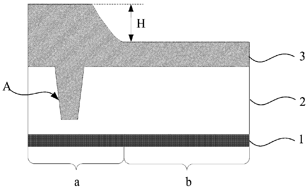
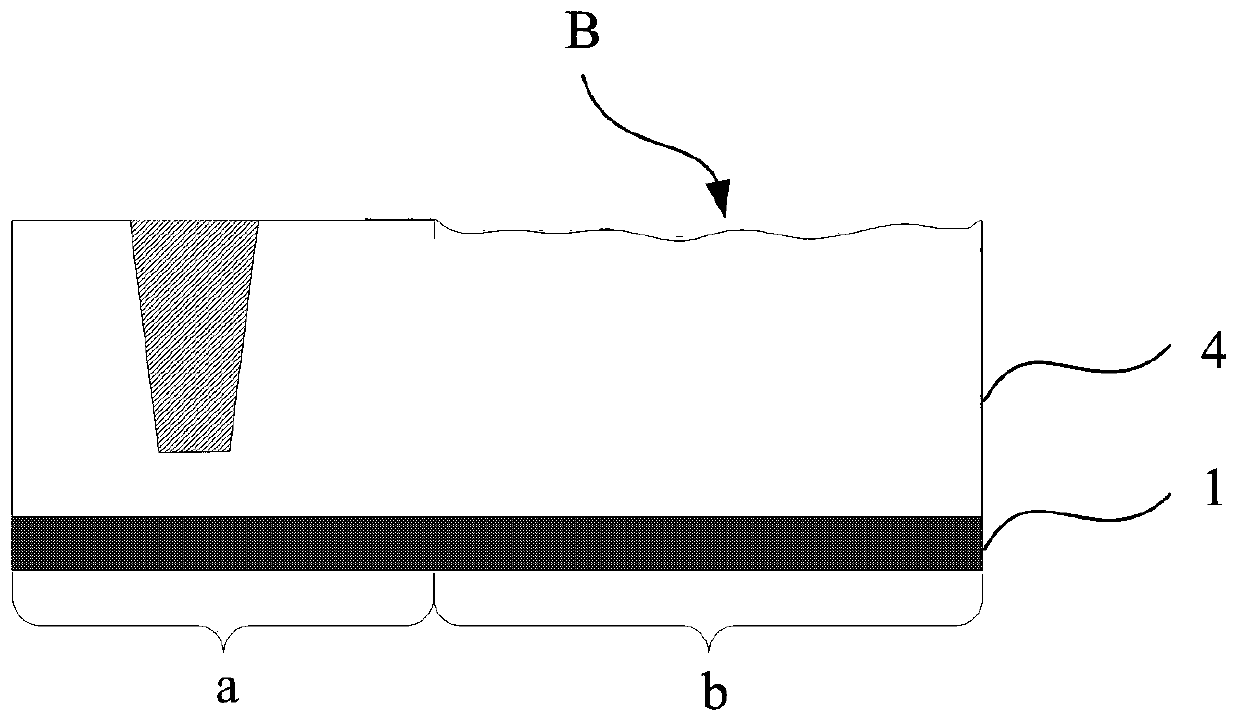
[0030] As described in the background art, in the related art, when forming a metal interconnection layer, it is usually provided such as figure 1 A semiconductor substrate 1 is shown and an insulating layer 2 formed on the semiconductor substrate 1, wherein the semiconductor substrate 1 defines a groove area a and a flat area b. And, a groove A is also formed in a portion of the insulating layer 2 corresponding to the groove region a. After that, a copper layer 3 is electroplated on the insulating layer 2 , so that the copper layer 3 fills the groove A. The semiconductor substrate 1 is then ground by a grinding process, and the copper layer above the insulating layer 2 is ground away to expose the surface of the insulating layer 2, thereby preparing a metal interconnection layer.

[0031] However, in the related art, when the copper layer 3 is electroplated, since the copper layer 3 needs to fill the groove A, the growth rate of the copper layer corresponding to the groove A...


PUM


Abstract

The invention provides a manufacturing method for a metal interconnection layer, and the method comprises the steps: providing a semiconductor substrate which is provided with at least one groove; forming a metal layer on the semiconductor substrate, the metal layer filling the groove and protruding upwards from the groove to a first height, the metal layer also covering the top surface of the semiconductor substrate, the top position of the top surface of the semiconductor substrate covered in the metal layer corresponding to the position of the second height, and the first height being higher than the second height; and etching at least the part, corresponding to the upper part of the groove, of the metal layer so that the top position of the part, corresponding to the upper part of thegroove, of the metal layer is lowered to the position of a third height, and the height difference between the third height and the second height is smaller than the height difference between the first height and the second height. According to the manufacturing method for the metal interconnection layer, the resistance characteristic and the stability of the finally manufactured metal interconnection layer can be ensured.

Description

technical field [0001] The invention relates to the technical field of semiconductor manufacturing, in particular to a method for manufacturing a metal interconnection layer. Background technique [0002] In the process of fabricating semiconductor devices, it is often necessary to form metal interconnect layers to connect different layers. [0003] In the related art, a method for forming a metal interconnection layer specifically includes: providing a semiconductor substrate, the semiconductor substrate having a groove area and a flat area, forming a groove on a portion of the semiconductor substrate corresponding to the groove area, and then forming a groove on the semiconductor substrate. A copper layer is deposited in the semiconductor substrate so that the copper layer fills the groove, and then the copper layer is ground by a grinding process to expose the surface of the semiconductor substrate, thereby forming a metal interconnection layer. [0004] However, in the ...

Claims


Application Information

Patent Timeline
Patent Type & Authority Applications(China)
IPC IPC(8): H01L21/48
CPCH01L21/4846
Inventor 张纪稳张玉贵崔助凤
Owner NEXCHIP SEMICON CO LTD
Why Eureka
Try Eureka