Display panel and manufacturing method thereof

A technology of display panel and manufacturing method, applied in semiconductor/solid-state device manufacturing, nanotechnology for materials and surface science, semiconductor devices, etc., can solve problems such as unfavorable display, high surface reflectivity, low contrast, etc. The effect of reducing the transmittance, enhancing the transmittance, and increasing the transmittance

Pending Publication Date: 2020-06-19
WUHAN CHINA STAR OPTOELECTRONICS SEMICON DISPLAY TECH CO LTD
View PDF12 Cites 9 Cited by
  • Summary
  • Abstract
  • Description
  • Claims
  • Application Information

AI Technical Summary

Problems solved by technology

However, compared with polarizers, the surface reflectance of color film technology is higher, and the contrast ratio under strong light is lower, which is not conducive to outdoor display

Method used


Image

  • Display panel and manufacturing method thereof
  • Display panel and manufacturing method thereof
  • Display panel and manufacturing method thereof

Examples


Embodiment Construction

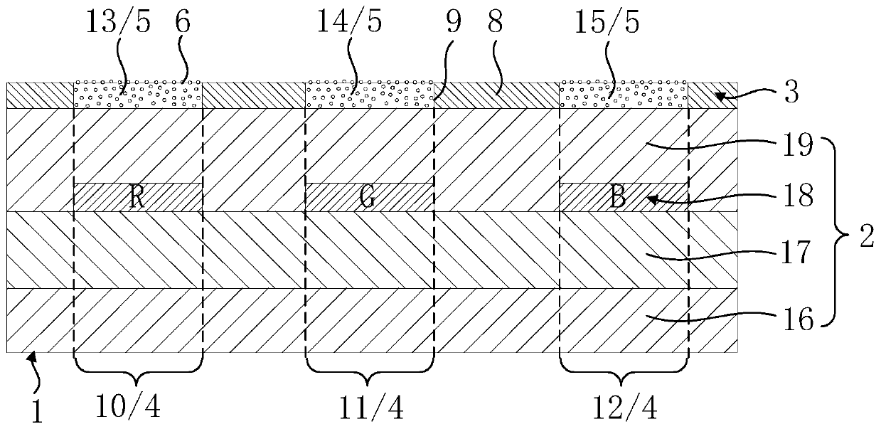
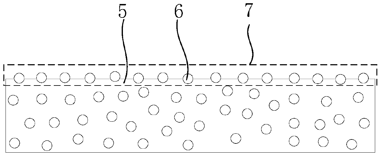
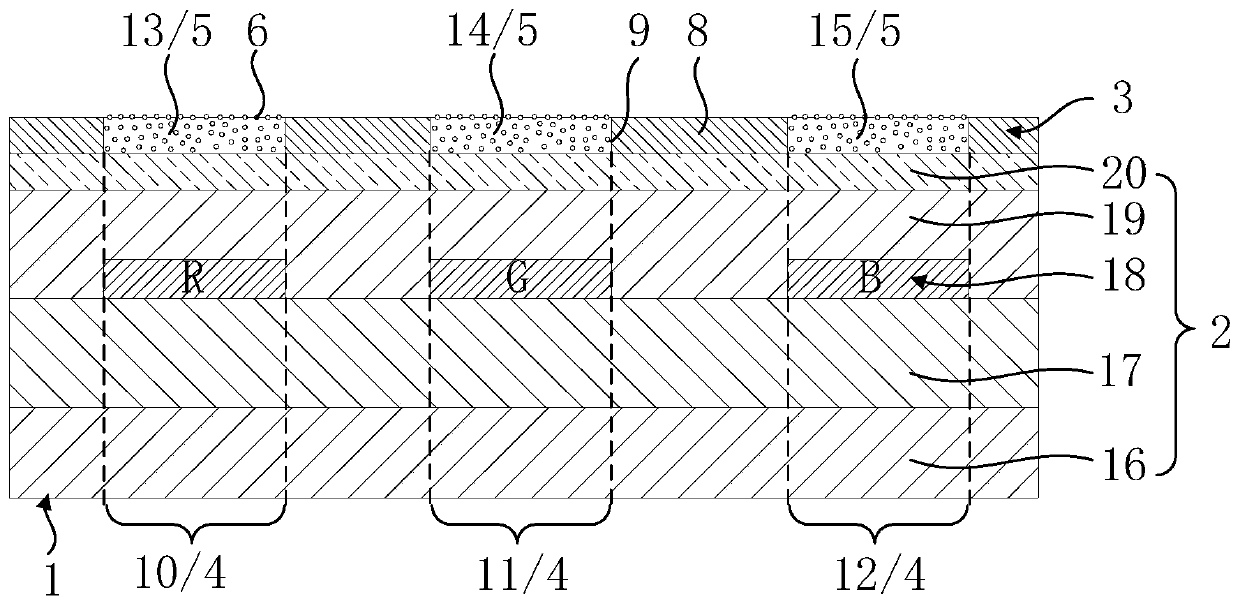
[0034] The technical solutions in the embodiments of the present application will be clearly and completely described below in conjunction with the drawings in the embodiments of the present application. Apparently, the described embodiments are only some of the embodiments of this application, not all of them. Based on the embodiments in this application, all other embodiments obtained by those skilled in the art without making creative efforts belong to the scope of protection of this application.

[0035] In the description of the present application, it should be understood that the terms "center", "longitudinal", "transverse", "length", "width", "thickness", "upper", "lower", "front", " Orientation indicated by rear, left, right, vertical, horizontal, top, bottom, inside, outside, clockwise, counterclockwise, etc. The positional relationship is based on the orientation or positional relationship shown in the drawings, which is only for the convenience of describing the a...


PUM

PropertyMeasurementUnit
diameteraaaaaaaaaa

Abstract

The invention discloses a display panel and a manufacturing method thereof. The display panel comprises a display device and an anti-reflection layer arranged on the display device. The display devicecomprises a plurality of sub-pixel areas distributed in an array; the anti-reflection layer comprises organic light-transmitting thin films arranged corresponding to the sub-pixel areas; the organiclight-transmitting thin films are doped with inorganic nano particles, and the inorganic nano particles located on the sides, away from the display device, of the organic light-transmitting thin filmsprotrude on the surfaces of the organic light-transmitting thin films to form nano moth eye structures. According to the invention, the anti-reflection capability of the display panel can be improvedby the anti-reflection layer, and the contrast ratio of the display panel is effectively improved.

Description

technical field [0001] The present application relates to the technical field of display panels, in particular to a display panel and a manufacturing method thereof. Background technique [0002] OLED (Organic Light Emitting Display, organic light emitting diode) display technology is becoming more and more mature, and the form of related products has gradually transitioned from rigid to foldable, and even to rollable and stretchable display products. OLED display technology makes the design of display products diversified and three-dimensional, and is increasingly developing in the direction of thinner, lighter, lower power consumption, and higher reliability. Under the premise of satisfying the OLED display performance, how to minimize the thickness of the display module is a difficult problem that needs to be overcome at present. [0003] Currently, OLED display products adopt a top-emitting device structure design in the field of mobile display to obtain a display effec...

Claims


Application Information

Patent Timeline
Patent Type & Authority Applications(China)
IPC IPC(8): H01L27/32H01L51/52H01L21/77H01L27/15B82Y30/00B82Y40/00H01L33/44
CPCH01L27/156B82Y30/00B82Y40/00H01L33/44H01L2933/0025H10K59/35H10K59/12H10K50/86H10K50/865H10K59/1201H01L25/0753H10K59/8791H10K2102/331H10K59/38H10K59/352H10K59/8792H10K59/353H10K71/135H10K59/873
Inventor 龚文亮鲜于文旭
Owner WUHAN CHINA STAR OPTOELECTRONICS SEMICON DISPLAY TECH CO LTD
Why Eureka
Try Eureka