Flexible array substrate, preparation method thereof and flexible display panel
A flexible array and substrate technology, applied in the direction of identification devices, instruments, semiconductor devices, etc., can solve the problems of stress and concentration that are easy to form long grooves
- Summary
- Abstract
- Description
- Claims
- Application Information
AI Technical Summary
Problems solved by technology
Method used
Image

Examples
Embodiment 1
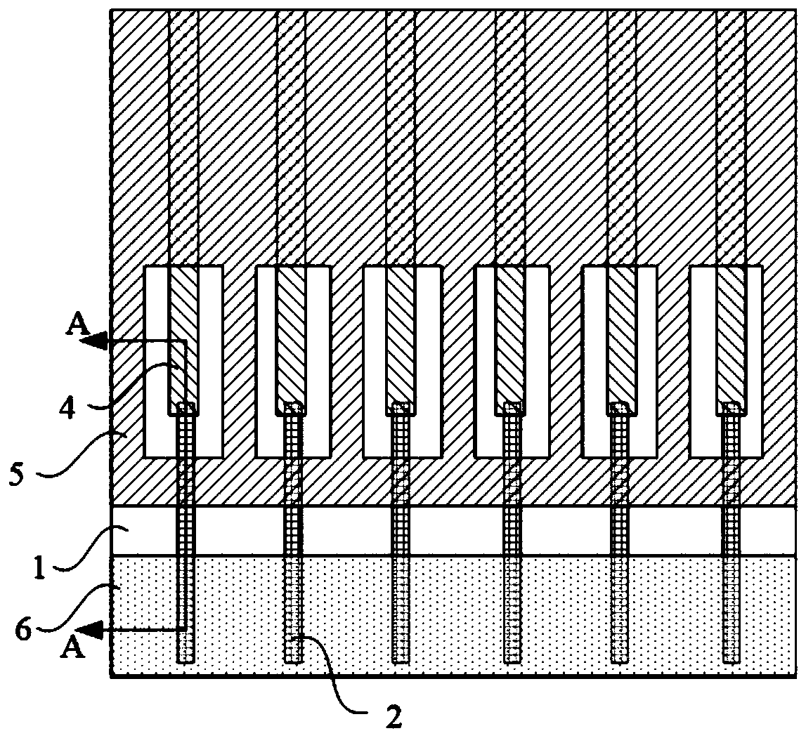
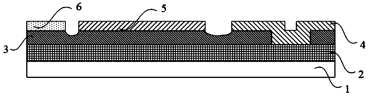
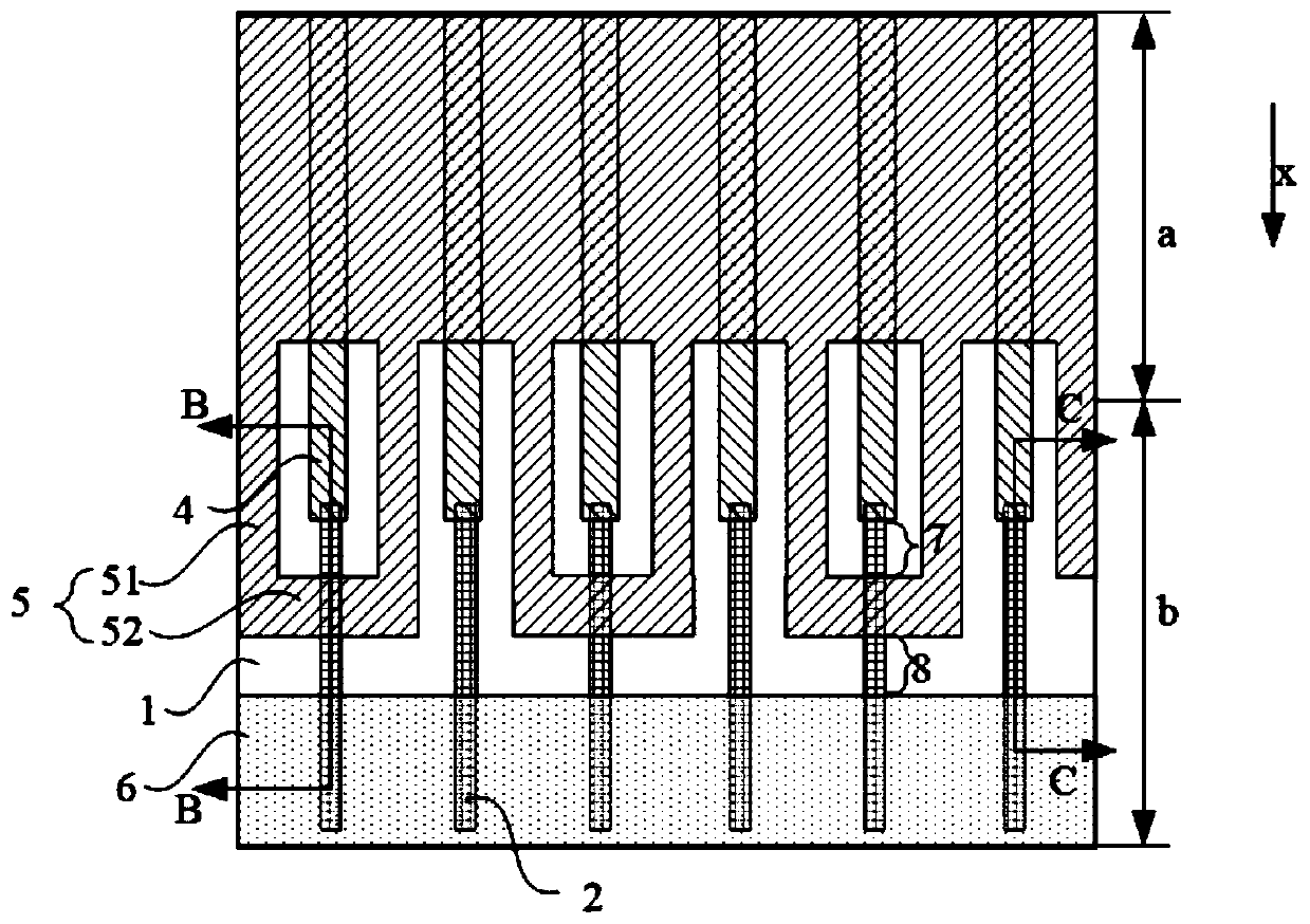
[0041] Such as Figure 2 to Figure 5 As shown, this embodiment provides a flexible array substrate, which has a display area a and a bending area b (Bending area) connected to the display area a. The flexible array substrate includes:
[0042] flexible substrate 1;
[0043] A plurality of first wires 2 located on the flexible substrate 1, the plurality of first wires 2 are parallel to the first direction, and the projections of the plurality of first wires 2 on the flexible substrate 1 are arranged in sequence along a direction perpendicular to the first direction , the first direction is the direction that the display area a points to the bending area b (such as figure 2 , 4 , arrow x shown in 5);
[0044] The first insulating layer 3 is located on the side of the first wire 2 away from the flexible substrate 1, the first insulating layer 3 has a plurality of first via holes 31, and the first via holes 31 are located in the bending region b;
[0045] A plurality of secon...
Embodiment 2
[0067] Such as Figure 2 to Figure 5 As shown, this embodiment provides a method for preparing a flexible array substrate, based on the flexible array substrate of Embodiment 1, the preparation method includes:
[0068] S11 , forming a plurality of first wires 2 on the flexible substrate 1 .
[0069] Wherein, the first conductive wires 2 can be formed in two steps, that is, the odd-numbered first conductive wires 2 are formed first, and then the even-numbered first conductive wires 2 are formed, so that crosstalk between adjacent first conductive wires 2 can be avoided.
[0070] S12 , forming a first insulating layer 3 on a side of the first wire 2 away from the flexible substrate 1 .
[0071] Wherein, the first insulating material layer may be formed on the side of the first wire 2 away from the flexible substrate 1 first, and then the first insulating material layer is patterned to form the first insulating layer 3 with the first via hole 31 .
[0072] S13 , forming a seco...
Embodiment 3
[0079] Such as Image 6 As shown, this embodiment provides a flexible display panel, including the flexible array substrate of Embodiment 1, and the flexible array substrate can be bent at the bending region b.
[0080] Wherein, since the flexible substrate in the flexible display panel of this embodiment is bendable, the flexible array substrate is bendable in the bending area b, so that the structure located in the bending area b can be bent to the flexible array The back side of the substrate can increase the proportion of the entire screen where the display area a of the flexible display panel is located, that is, increase the screen-to-body ratio.
[0081] Specifically, the flexible display panel can be any product or component with a display function such as an organic light emitting diode (OLED) display panel, electronic paper, mobile phone, tablet computer, television, monitor, notebook computer, digital photo frame, and navigator.
PUM
 Abstract
Description
Claims
Application Information
 - R&D
- Intellectual Property
- Life Sciences
- Materials
- Tech Scout
- Unparalleled Data Quality
- Higher Quality Content
- 60% Fewer Hallucinations
Browse by: Latest US Patents, China's latest patents, Technical Efficacy Thesaurus, Application Domain, Technology Topic, Popular Technical Reports.
© 2025 PatSnap. All rights reserved.Legal|Privacy policy|Modern Slavery Act Transparency Statement|Sitemap|About US| Contact US: help@patsnap.com