Semiconductor laser device bar cleavage epitaxial wafer adhering device and semiconductor laser device bar cleavage epitaxial wafer adhering method

A chip device and laser technology, applied in the structural details of semiconductor lasers and other directions, can solve the problems of insufficient contact between the blue film and the epitaxial wafer, affecting the cleavage effect of the epitaxial wafer, and insufficient expansion of the blue film, etc., to achieve operation and inspection. Convenient and reliable, good patch effect, simple structure

Active Publication Date: 2020-07-03
潍坊华光光电子有限公司
View PDF4 Cites 0 Cited by
  • Summary
  • Abstract
  • Description
  • Claims
  • Application Information

AI Technical Summary

Problems solved by technology

When patching, it is required that the blue film must be fully expanded and tightened on the square frame. The epitaxial film should be pasted on the blue film to be smooth. The blue film is uneven, and when the epitaxial wafer is pasted on it, the epitaxial wafer cannot fully contact with the blue film, resulting in uneven stress on the epitaxial wafer during strip cleavage, causing breakage and chipping of the cleaved strip, and even The strips produced by cleavage of the entire epitaxial wafer are unqualified
[0003] At present, the commonly used patch method is to directly paste the blue film on a fixed-size square frame by hand, and then place the epitaxial wafer in the middle of the blue film with tweezers. This method is simple to operate, but the blue film is directly pasted. On the frame, it often occurs that the expansion of the blue film is insufficient and the stretching is not tight, so that the entire blue film is not evenly pasted on the frame, and when the epitaxial wafer is pasted on the blue film, the blue film and the epitaxial wafer cannot be fully contacted, thereby affecting the epitaxial film. chip cleavage effect

Method used


Image

  • Semiconductor laser device bar cleavage epitaxial wafer adhering device and semiconductor laser device bar cleavage epitaxial wafer adhering method
  • Semiconductor laser device bar cleavage epitaxial wafer adhering device and semiconductor laser device bar cleavage epitaxial wafer adhering method
  • Semiconductor laser device bar cleavage epitaxial wafer adhering device and semiconductor laser device bar cleavage epitaxial wafer adhering method

Examples


Embodiment 1

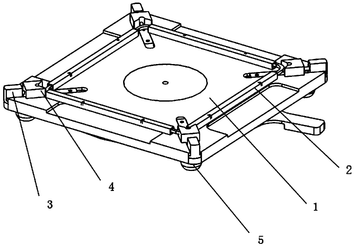
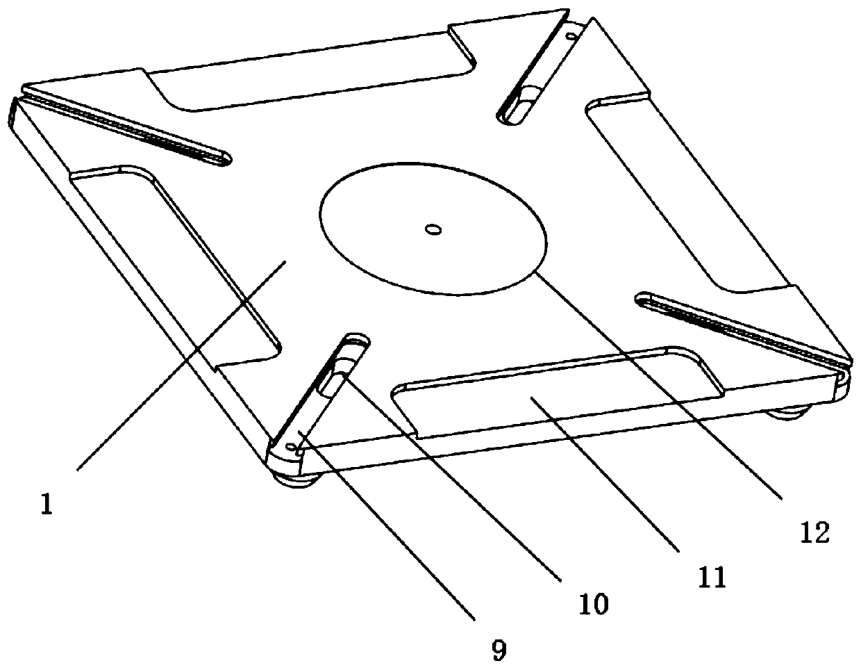
[0046] Such as Figure 1-11 As shown, a semiconductor laser bar cleavage epitaxial wafer placement device includes a main body 1, a square frame 2, a round cake 6, a positioning block 3 and a sliding block, the square frame 2 is located on the upper part of the main body 1, and the round cake 6 is located on the main body 1 In the lower part, the main body 1 has a square structure, and the four corners of the main body 1 are provided with chutes 9 towards the center. The four chutes 9 have the same structural size. The positioning blocks 3 are fixed on the four corners of the main body 1. Located at the upper end of the chute 9, the sliding block is located in the chute 9 and can slide along the chute 9;

[0047] The middle part of the round cake 6 is provided with a fixing hole 20, and the pin shaft 7 passes through the fixing hole 20 to connect the round cake 6 and the main body 1. The round cake 6 can rotate relative to the main body 1 through the pin shaft 7, and the round...

Embodiment 2

[0050] A semiconductor laser bar cleavage epitaxial chip placement device, the structure is as shown in Embodiment 1, the difference is that the bottom of the positioning block 3 is provided with a slide rail II18, and the middle position of the bottom of the slide rail II18 is provided with a screw hole 17, and the screw The hole 17 is used to fix the position of the positioning block 3 on the main body 1, and one end of the positioning block 3 is provided with a positioning rod 16, and the positioning rod 16 is used for positioning the sliding block.

Embodiment 3

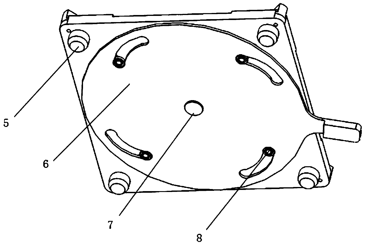
[0052] A semiconductor laser bar cleavage epitaxial chip placement device, the structure is as shown in Embodiment 1, the difference is that the guide groove 21 is a long arc-shaped hole, and the two ends of the long arc-shaped hole are provided with a first arc 31 and the second arc 32, as Image 6 As shown, the direction of the arrow is counterclockwise, and the distance from the first arc 31 to the center of the round cake 6 is smaller than the distance from the second arc 32 to the center of the round cake 6 .

[0053] The slider includes a slider main body 4 and a slide rail I14 located at the lower part of the slider main body 4. The slide rail I14 is integrated with the slider main body 4. The size of the slide rail I14 is adapted to the size of the chute 9. The size of the slider main body 4 One end is provided with the positioning hole 13 that cooperates with positioning rod 16, and the other end is provided with V-shaped groove 15; The positioning rod 16 cooperates ...


PUM


Abstract

The invention relates to a semiconductor laser device bar cleavage epitaxial wafer adhering device and a semiconductor laser device bar cleavage epitaxial wafer adhering method, and belongs to the technical field of semiconductor laser device chips. The device comprises a main body, a square frame, a round cake, positioning blocks and sliding blocks, wherein the square frame is located on the upper portion of the main body, the round cake is located on the lower portion of the main body, the main body is of a square structure, sliding grooves facing the center are formed in the four corners ofthe main body respectively, the positioning blocks are fixed to the four corners of the main body, the sliding blocks are located in the sliding grooves and can slide along the sliding grooves, the middle of the round cake is connected with the main body through a pin shaft, four guide grooves with the same structure are formed in the positions, close to the edge, of the round cake and used for guiding the sliding blocks to slide in the sliding grooves respectively, the square frame is of an inside-outside telescopic structure, and one end of the sliding block abuts against the corner of thesquare frame and is used for pushing the square frame to contract. The device has an automatic expansion function, and is simple in structure, convenient to operate and check, good in chip adhering effect and high in production efficiency.

Description

technical field [0001] The invention relates to a semiconductor laser bar cleavage epitaxial wafer patching device and a patching method, belonging to the technical field of semiconductor laser chips. Background technique [0002] Due to the advantages of small size, light weight, high electro-optical conversion efficiency, long life and high reliability, semiconductor lasers (LDs) have gradually replaced the use of gas and solid-state lasers in the fields of communication, medical treatment, display, industrial production and security. Its scope of application is gradually expanding. In the production process of semiconductor lasers, it is necessary to go through multiple processes. First, the epitaxial furnace is used to grow high-quality LD epitaxial wafers, and then the LD epitaxial wafers are subjected to PECVD deposition, photolithography, electrode fabrication and other processes to make a single epitaxial wafer Capable of producing thousands of semiconductor laser c...

Claims


Application Information

Patent Timeline
Patent Type & Authority Applications(China)
IPC IPC(8): H01S5/02
CPCH01S5/02
Inventor 张广明汤庆敏赵克宁贾旭涛刘丽青
Owner 潍坊华光光电子有限公司
Why Eureka
Try Eureka