
Resistive memory device and programming method of the same

A technology of resistive memory and programming method, which is applied in the direction of static memory, digital memory information, information storage, etc., and can solve the problems of degrading the performance of resistive memory devices, etc.

Active Publication Date: 2020-07-07
SAMSUNG ELECTRONICS CO LTD
View PDF9 Cites 4 Cited by
  • Summary
  • Abstract
  • Description
  • Claims
  • Application Information

AI Technical Summary

Problems solved by technology

However, the resistance of a programmed resistive memory cell may drift or vary over time, which can degrade the performance of the resistive memory device

Method used


Image

  • Resistive memory device and programming method of the same
  • Resistive memory device and programming method of the same
  • Resistive memory device and programming method of the same

Examples


Embodiment Construction

[0028] Hereinafter, various example embodiments will be described more fully with reference to the accompanying drawings, in which some example embodiments are shown. In the drawings, like numerals designate like elements throughout. The description of certain aspects of one figure may be omitted from the description of other figures.

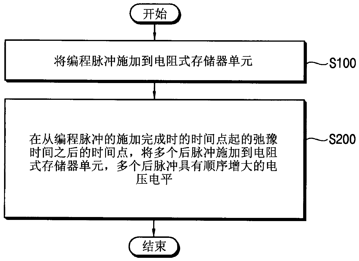
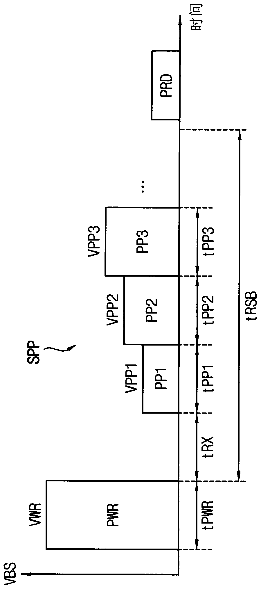
[0029] figure 1 is a flowchart illustrating a programming method of a resistive memory device according to example embodiments, figure 2 is a timing diagram illustrating a programming method of a resistive memory device according to example embodiments. exist figure 2 , the horizontal axis represents time, and the vertical axis represents the bias voltage VBS applied to the resistive memory cell.

[0030] refer to figure 1 and figure 2 , the programming pulse PWR is applied to the resistive memory cell (S100), and at a time point after a relaxation time (relaxation time) tRX from the time point when the application of the programming p...


PUM


Abstract

Resistive memory device and programming method of the same. In some example embodiments, a program pulse is applied to a resistive memory cell and a plurality of post pulses are applied to the resistive memory cell at a time point after a relaxation time from a time point when application of the program pulse is finished, the plurality of post pulses having voltage levels that increase sequentially. Programming speed and / or performance of the resistive memory device may be enhanced by accelerating resistance drift of the resistive memory cell using the plurality of post pulses having the voltage levels that increase sequentially.

Description

[0001] This application claims priority from Korean Patent Application No. 10-2018-0173853 filed on December 31, 2018 at the Korean Intellectual Property Office (KIPO), the disclosure of which is hereby incorporated by reference in its entirety. technical field [0002] Some example embodiments relate generally to semiconductor integrated circuits, and more particularly, resistive memory devices and / or methods of programming resistive memory devices. Background technique [0003] Semiconductor memory devices for storing data can be classified into volatile memory devices and nonvolatile memory devices. Volatile memory devices, such as dynamic random access memory (DRAM) devices, are generally configured to store data by charging or discharging capacitors in memory cells, and lose the stored data when power is turned off. Nonvolatile memory devices such as flash memory devices can retain stored data even when power is turned off. Various types of resistive memory have been d...

Claims


Application Information

Patent Timeline
Patent Type & Authority Applications(China)
IPC IPC(8): G11C13/00
CPCG11C13/0004G11C13/0021G11C13/0097G11C13/0069G11C2013/0092G11C13/003G11C2213/76G11C2213/72G11C2213/82G11C2213/79G11C2213/15G11C13/0033G11C13/0035G11C13/0061G11C2013/0078G11C13/0038
Inventor 曺溶成金武星白承柔白钟民郑凤吉
Owner SAMSUNG ELECTRONICS CO LTD
Learn More