An Ultra-Wideband Helical Laminated Absorber

A helical, ultra-broadband technology, applied in instruments, antennas, optics, etc., can solve the problems of limited application, narrow frequency band, high density, etc., to achieve the effect of diverse functions, reducing reflection and scattering, and flexible design

Active Publication Date: 2022-01-25
NANJING UNIV OF POSTS & TELECOMM
View PDF5 Cites 0 Cited by
  • Summary
  • Abstract
  • Description
  • Claims
  • Application Information

AI Technical Summary

Problems solved by technology

However, traditional absorbing materials have shortcomings such as narrow frequency band, high density, and low performance, which limit their application in micro-nano photonics devices.

Method used


Image

  • An Ultra-Wideband Helical Laminated Absorber
  • An Ultra-Wideband Helical Laminated Absorber
  • An Ultra-Wideband Helical Laminated Absorber

Examples


Embodiment 1

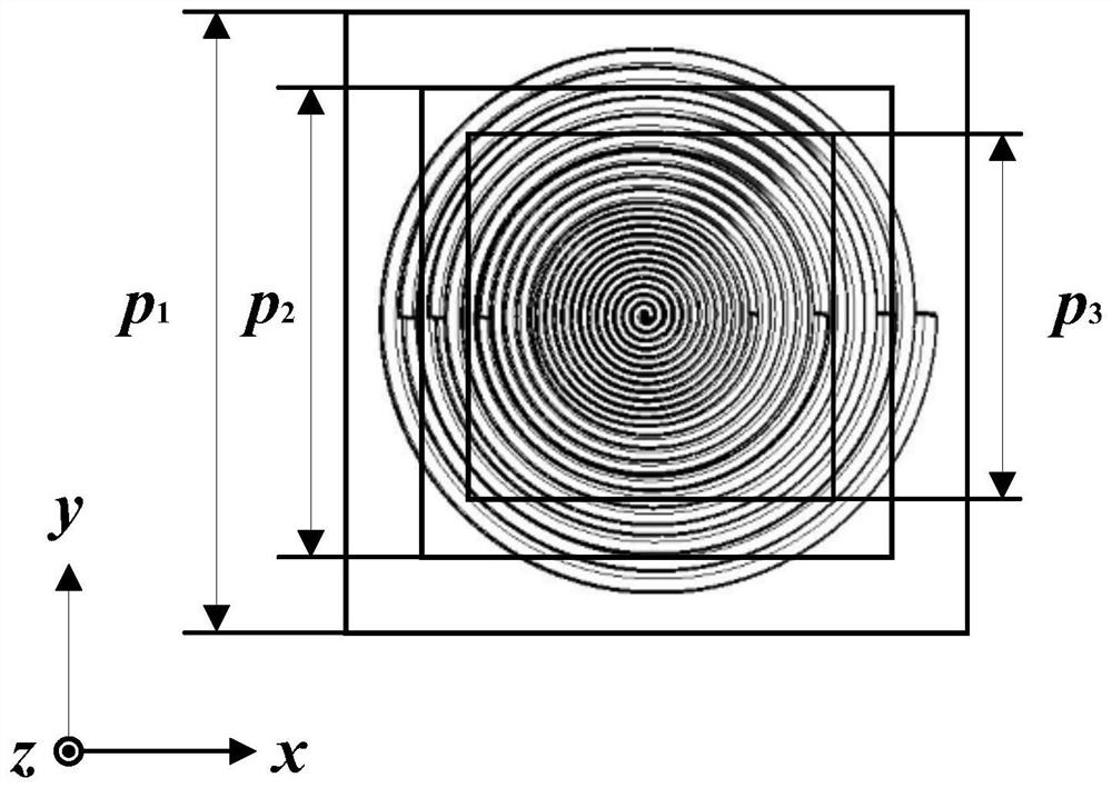
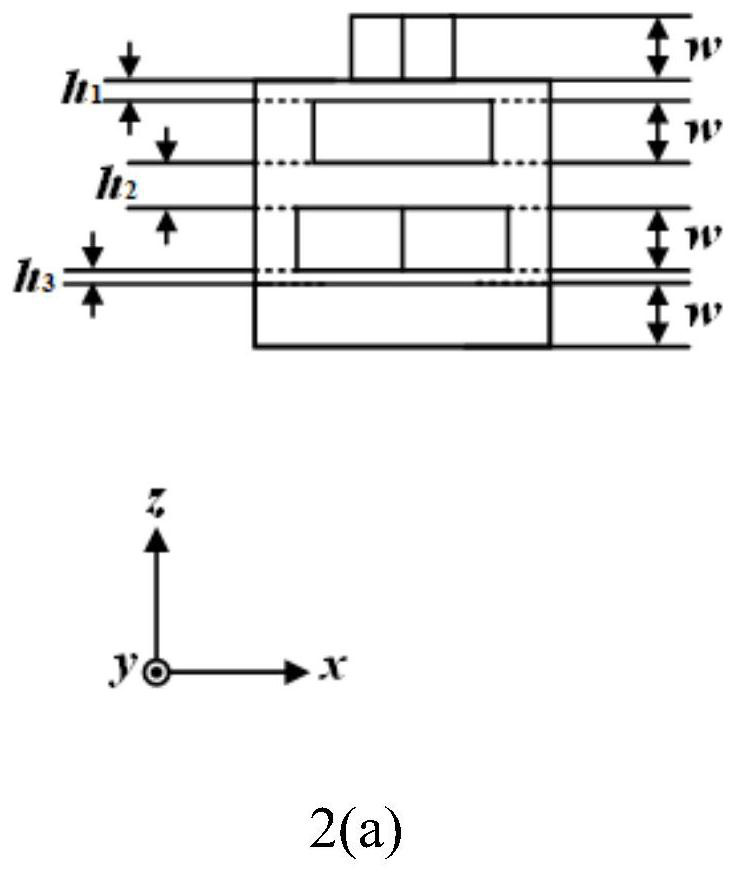
[0033] Embodiment one, as image 3 As shown in (a), an ultra-broadband spiral laminated absorber includes: a metal reflective layer is arranged on the bottom layer, and an ultra-wideband spiral laminated absorber is arranged on the metal reflective layer. In this embodiment, the ultra-wideband spiral laminated absorber The unit includes a layer of dielectric layer, the top layer of Archimedes spiral metal structure is set on the dielectric layer, and two layers of Archimedes spiral metal structure are embedded in the medium layer; all Archimedes spiral metal structures can be moved from the bottom layer to the The top layer is divided into a pyramid structure with the same number as the medium layer. The side view of this embodiment is as figure 2 As shown in (a), where optionally, the distance between the bottom metal reflector and the first layer of Archimedes spiral from bottom to top h 3 =20 nm, the distance between the first layer of Archimedes spiral and the second l...

Embodiment 2

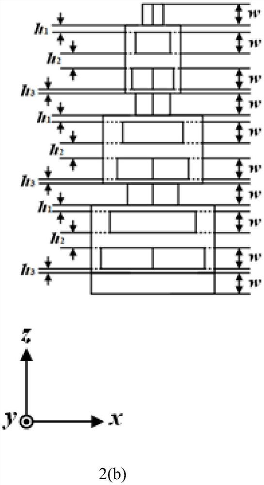
[0034] Embodiment two, such as image 3 As shown in (b), an ultra-wideband spiral laminated absorber includes: a metal reflective layer is arranged on the bottom layer, and an ultra-wideband spiral laminated absorber is arranged on the metal reflective layer. In this embodiment, the ultra-wideband spiral laminated absorber The wave unit includes a first dielectric layer, a second dielectric layer and a third dielectric layer arranged from the bottom layer to the top layer, the first dielectric layer is arranged on the metal reflective layer, and the absorber has a total of nine layers from bottom to top. The Mead spiral metal structure includes two layers of Archimedes spiral metal structures embedded in the first dielectric layer starting from the bottom layer, and a layer of Archimedes spiral metal structures is arranged between the first dielectric layer and the second dielectric layer, and The two-layer Archimedes spiral metal structure embedded in the first medium layer a...

Embodiment 3

[0038] Embodiment 3. An ultra-broadband helical laminated wave absorber. The three-dimensional view of the embodiment is as follows image 3 As shown in (c), the side view is as figure 2 As shown in (c), this embodiment includes a metal reflective layer arranged on the bottom layer, and an ultra-broadband spiral laminated absorbing unit is arranged on the metal reflective layer. In this embodiment, the ultra-wideband spiral laminated absorber, such as image 3 (c) and figure 2 As shown in (c), the unit structure of the ultra-broadband spiral laminated absorbing unit includes a pyramid-shaped medium composed of the first dielectric layer 12, the second dielectric layer 11 and the third dielectric layer 10, and the first dielectric layer 12 set on the metal reflective layer 13. The first to nine layers of spiral resonance structures 1, 2, 3, 4, 5, 6, 7, 8, 9 (that is, the Archimedes spiral resonance structure, hereinafter referred to as the spiral structure or Archimedes spi...


PUM

PropertyMeasurementUnit
thicknessaaaaaaaaaa

Abstract

The invention discloses an ultra-wideband spiral laminated wave absorber, which comprises: a metal reflective layer is arranged on the bottom layer, and at least one ultra-wideband spiral laminated wave absorber is arranged on the metal reflective layer. When the ultra-wideband spirally laminated wave absorber is more than One, all ultra-broadband spiral laminated absorbing units adopt the same structure and are arranged equidistantly on the metal reflective layer; the ultra-broadband spiral laminated absorbing unit includes at least one dielectric layer, and the top layer of Archimedes is arranged on the top dielectric layer A spiral metal structure, wherein at least two layers of Archimedes spiral metal structures are embedded in each dielectric layer; if there are more than one dielectric layer, all dielectric layers are arranged in a pyramid from the bottom dielectric layer to the top dielectric layer; all A The Kimedean spiral metal structure can be divided into individual pyramid structures with the same number of dielectric layers from the bottom layer to the top layer. The absorption frequency of the wave absorber provided by the invention can span three frequency bands of infrared, visible light and ultraviolet.

Description

technical field [0001] The invention belongs to the technical field of wireless communication and microwave devices, in particular to the design field of wave-absorbing devices that can span multiple frequency bands, and specifically relates to an ultra-broadband spiral laminated wave absorber. Background technique [0002] With the rapid development of modern science and technology, satellite communications, radar detection, radio broadcasting, and thermal imagers, which use electromagnetic waves as the medium for signal and energy transmission, are widely used. At the same time, the negative impact of electromagnetic wave radiation on the environment is also increasing. For example, electromagnetic wave interference will delay the normal take-off of aircraft, affect the quality of communication, interfere with the normal operation of instruments, and electromagnetic wave radiation will also affect human health. Therefore, it is becoming more and more important to control e...

Claims


Application Information

Patent Timeline
Patent Type & Authority Patents(China)
IPC IPC(8): H01Q17/00G02B1/00G02B5/00
CPCH01Q17/008G02B1/002G02B5/003
Inventor 章海锋曾立
Owner NANJING UNIV OF POSTS & TELECOMM
Why Eureka
Try Eureka